So we’re off to part two of my teardown of the transistor clock and things are getting complicated.
Really complicated…
Goal
Last time, I covered the first stage of the clock that left us with a 9V DC rail and a 60Hz square wave. The challenge for today is to turn that 60Hz square wave into a 1Hz square wave that will be used as the clock’s “pendulum”. This will involve the introduction of a few new subcircuits a fairly complicated timing diagram.
Put On Your Flip Flops
A Flip-flop is an electronic circuit that is sometimes referred to as a “bi-stable circuit”. “Bi-stable” means that it has two possible states and can alternate between them. In simplest terms, a flip-flop is a storage device that can store a single bit of information (0 or 1). There are a number of different types of flip flops that vary on how they output information and how their state is changed. Our circuit will be using a T-flip-flop.
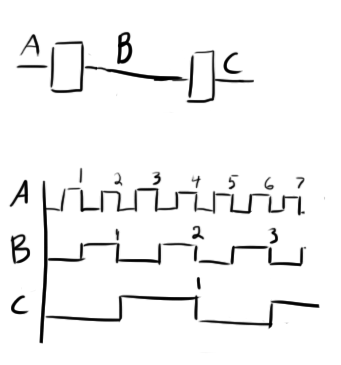
A T-flip-flop alternates state every time its input trigger is pulsed. For our purposes, it looks something like this:
This device will be useful to us because it will allow us to divide the frequency of a clock signal by two. Think of it this way: a clock pulse consists of an up and down swing. Let’s say we trigger a T flip-flop on the down swing of its input. If its output starts low, on the first high to low transition of the input, its output will go high, on the second high to low transition, its output will go low.
This will halve the input frequency.
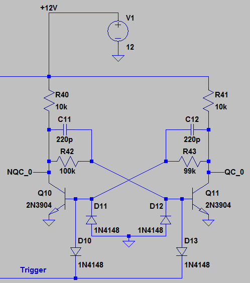
In its current configuration, the flip-flop is not triggered by a downward clock edge but instead by a brief low pulse on the line connected to D10 and D13 (this line is otherwise held high). It has two outputs QC_0 and NQC_0. QC_0 is considered our regular output, and NQC_0 is the inverted output (“N” means “Not”). Note that this assignment is arbitrary. The point is that the two outputs alternate being high and low, so whichever you like to pick as your regular output is up to you. The other output will always be the inverse.
Now, analyzing bistable circuits is always kind of odd because you naturally want to think about what happens at the very beginning when you turn it on. It becomes very difficult if you take this approach, because you will find two things happening simultaneously in parallel and you will have trouble deciding which one will “win”.
A “bi-stable” circuit is just that, it’s only stable in two different states, all other states are unstable and considered impossible. The problem is that in a mathematically perfect world with zero noise, a bi-stable circuit started at rest would remain in an indeterminate state forever (imagine a coin balanced perfectly on its edge). This is a problem that you might run into when you use a circuit simulator like LTSpice. Rather than choosing one side or the other, LTSpice will be happy to keep the circuit in an indeterminate state. You’ll note that R43 is 99k while its twin R42 is 100k. This is to give a tiny bit of preference to one state over the other to keep LTSpice from balancing on the edge.
The point is, as counter-intuitive as it may be, when analyzing a bistable circuit, you have to make the assumption that it is already in one of the two states when you begin your analysis. Don’t worry about what happened when you first turned on power. After any appreciable amount of time, some random factor (noise, non-perfect components, etc) will cause the coin to topple into one of these two states (heads or tails). Just assume it was always like that.
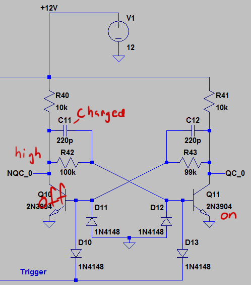
So what are our states? Let’s begin by looking at the state where QC_0 is low:
In this state, current passes through R42 and down to ground through the emitter of Q11 turning it on. Because Q11 is on, QC_0 is near ground, and no current can flow through the emitter of Q10 which therefore stays off. Because the emitter of Q11 acts like a diode, its base is at around .7V. This makes the voltage across C11 around 11V.
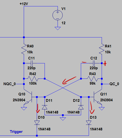
The circuit will stay in this state until it is triggered. The circuit is triggered when the trigger line drops close to zero. D13 has a slightly smaller forward voltage than Q11’s base-emitter junction, so as soon as the trigger gets close to zero, current will start to flow through D13 instead of Q11’s base. This will lower Q11’s base to around D13’s forward voltage which will start to turn the transistor off. At this point, the trigger pulse can rise again as it has already set events in motion that will cause the flip-flop to flip.
Slightly shutting off Q11 will lower the amount of current passing through R41 decreasing the voltage drop across that resistor. This will cause QC_0’s voltage to rise slightly. C12, which previously had 0V across it will start to build up a positive voltage. Remembering the formula for capacitors:
![]()
An increasing potential means that current will flow through C12 towards the base of Q10.
Current will also pass through R43, but over such a short time span, more charge will actually pass through the capacitor (The resistor is just there to maintain the new state once it is achieved). As current passes through the emitter of Q10, it will turn on slightly and NQC_0 will begin to drop. Remember that C11 is already charged to about 11V. As NQC_0 drops, the potential across C11 will begin to drop as well. Remembering the formula from before. A negative change in potential equates to a negative current:
This negative current will pull charges away from the base of Q11 which will turn it off even harder. In fact, if it weren’t for D12, the base of Q11 would go very negative and potentially cause damage.
So you’ve got a system where the harder Q10 turns on, the more charge you pull from Q11’s base and the harder you turn Q11 off. This is a positive feedback loop that will snap the circuit into the other state:
The whole secret to this transition is how long the trigger pulse is. After poking at the circuit in LTSpice for a while, I found that the pulse has to end some point before QC_0 has risen all the way. Basically, as long as the pulse is present, all of the current passing through C12 is just dropping through D10. Only after the pulse has ended can some of this charge pass into the base of Q10 and start to turn it on. If the pulse is still present when QC_0 reaches its maximum voltage, there will no longer be a
![]()
across C12, so little current will flow into Q10, and Q10 will remain off. Also, at this point, both sides will be in the exact same state basically resetting the flip-flop. Upon letting go, the flip-flop will randomly fall into one of the two states.
That represents the maximum trigger pulse length. Assuming that the trigger pulse drops all the way to zero, there really isn’t a minimum pulse length. You just need enough time to suck all of the charge out of whatever parasitic capacitance resides in Q11’s base. Assuming ideal components, there should be no minimum pulse length.
So how does one achieve the right pulse length? It’s actually quite simple:
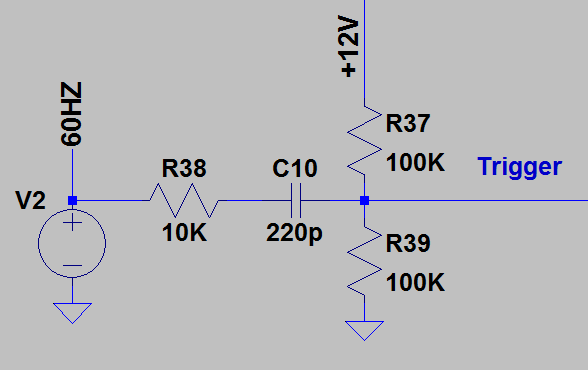
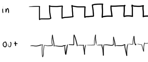
This simple high pass filter will turn the 60Hz square wave into a high and low pulse train. R37 and R39 will keep the trigger output at a nominal 6V until a clock edge. Let’s say for example that the clock is going from 12V to 0V. This will create a rapidly changing potential across C10. Because the potential is going from positive to negative, current through C10 will flow to the left. This will have the effect of lowering the trigger’s voltage and (as you saw above) pulling current out of the trigger diodes.
After this clock edge, current will flow through R37 and slowly bring the trigger voltage back to 6V. Because it’s focused around the clock edge and C10 is very small, this entire process happens very quickly and should produce a trigger of the right length to trip the flip-flop. When the clock goes from low to high, there will be a positive pulse on the trigger output, but this is ignored by the flip-flop’s input diodes.
So we have a device that will divide a frequency by two, a fundamental component in our prescaler. Now let’s figure out how to chain them together.
Timing
The fact that AC power runs at 60Hz in the US presents a problem. 60 is not a power of two. If power ran at 32Hz for example, we could just do this (note that
![]()
is the regular output and
![]()
is the inverted output):
Though I didn’t have a enough room to draw it, you can imagine how the 1Hz line would follow the pattern and be a 1/32 reduction of the original signal.
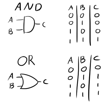
In order to get a division by 60, some special logic is going to have to be introduced. You might be familiar with simple logic gates:
An “AND” gate’s output goes high when both of its inputs are high while an “OR” gate’s output goes high when either of its inputs are high. If you have trouble with the symbols, just remember this:
I’ll be going over how to make these gates later, but for the time being, just remember what they’re supposed to do, and we should be able to get our 60Hz down to 1.
This 1/60 reduction will happen in two stages. First, we’ll be reducing by 1/10, and then again by 1/6. This will be useful as once we get our 1Hz clock, we’ll be reducing by 1/10 to get our 10 second’s place and then by 1/6 to get our one minute’s place. This process will continue for the 10 minute’s place and hours and so on. We can reuse this exact same topology in each of those cases.
Let’s start our 1/10 reduction with a simple scenario with 3 T-flip-flops in a series:
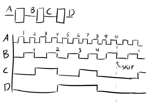
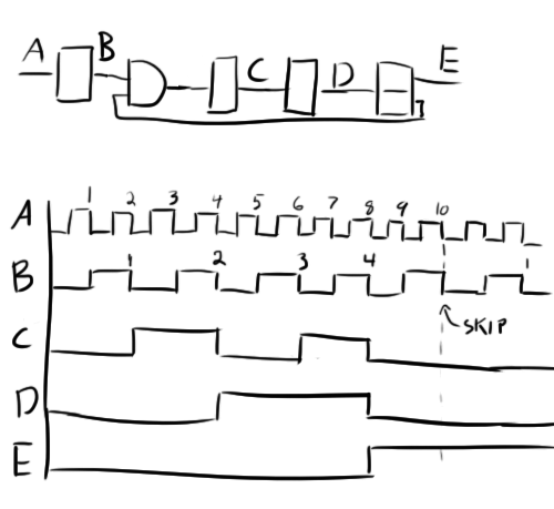
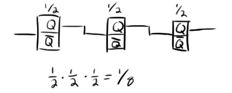 This will generate a 1/8 clock reduction which is a good start. We can’t add another flip-flop because that would give us a 1/16 reduction which is past our goal of 1/10. What we need to do now is add some logic that will slow down one of our flip flops. Basically, we need one of them to ignore a clock pulse every once in a while. For example, what if we made it so the middle flip flop ignored an incoming clock pulse after four pulses? (remember that the flip-flops are triggered by a high to low transition of a clock so a “pulse” is a high-low clock edge)
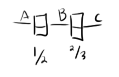
Now, for every 5 pulses of B, C only produces 2 pulses. This in effect changed a 1/2 reduction to a 2/5 reduction. Combining this with the other two flip-flops, you can multiply their reductions together:
![]()
Which is exactly what we want.
Okay, so how do we get the second flip-flop to ignore a clock pulse? The answer is to add an AND gate to its input and connect the output of the first flip flop to one of the AND gate’s inputs. The second input of the AND gate will act sort of like an enable pin for the second flip flop. If it’s high, any signal coming out of the first flip-flop will pass right through. When it’s low, the output will be low regardless of what the first flip-flop is doing.
Now the challenge is finding a signal that will disable the second flip flop after four pulses. Looking at the above timing diagram, you can imagine that if another flip-flop was fed the D signal, it would go high right when the 4th pulse appears on B. We could use the inverted version of this signal to control the second flip-flop.
So for the first three pulses,
![]()
is low and
![]()
is high, allowing B to pass to the second flip flop. As soon as
![]()
goes high though, the second flip-flop is disabled.
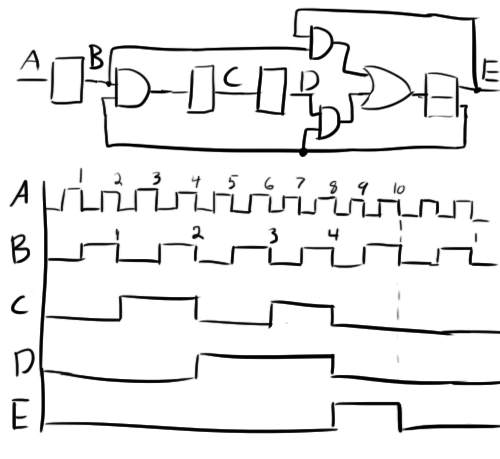
This presents a problem. Once the AND gate is turned off, there will be nothing to turn it back on again, and the second flip-flop will never see another pulse. To fix this, we need some way to reset the circuit and force E low again just after the first skipped pulse on B. We can actually use the B pulse itself to pull the E line low again and reactivate the second flip-flop. This can be done with an OR gate. We want a pulse on D OR B to toggle the 4th flip-flop.
Now this presents even more problems. We want the signal from B to trigger the 4th flip-flop, but only when E is high. In its current configuration, B will trigger the 4th flip-flop when we don’t expect it and cause all kinds of trouble.
This can be solved with (another) AND gate. This gate will make sure that B only triggers the 4th flip-flop when E is high. Otherwise, B’s contribution will be ignored:
Essentially, D turns E on, and B turns it off. Note that the final flip-flop is not dividing the frequency as E and D will flip the same number of times per cycle.
This configuration produced the clock signals drawn above perfectly in LTSpice, which is why I was concerned when I realized that there is still more to the circuit. I saw another AND gate, and I couldn’t figure out what it was for. I was really scratching my head on this problem for a while and even resorted to emailing the clock’s designer for help. Before he had a chance to get back to me though, I figured it out.
During startup, the flip-flops will all be in a random state. This state is dependent on uncontrollable factors such as slight differences in component values, temperature in the room, what day of the week it is, etc. There is one such random configuration that will actually freeze the clock if it’s left in this configuration.
If E is high upon startup, the AND gate on the left will be shut off, and no clock will make it to the second flip-flop. C and D will not change state. If D’s state happens to also be high from the start, it will be stuck high forever, and the output of the OR gate will be stuck high and never have a high to low transition. This means that the clock pulses coming in to the OR gate from the second AND gate will be ignored.
The reason it took me so long to find it is because my LTSpice model is in a mathematically perfect world, so it always picks the exact same startup state of its flip-flops. Because this state wasn’t the one mentioned above, I never saw its effects.
Fixing the problem is pretty trivial. All you need to do is make sure that D doesn’t get stuck high. This can be done by passing it through (yet another) AND gate with the other input coming from
![]()
. While
![]()
is high, the output of this new AND gate will be low regardless of where D is stuck.
(Try not to confuse the “D” with the AND gates!)
Now we’ve finally got the right setup. This combination of gates will give you everything you need to scale down the input signal by 1/10.
Next is the 1/6 reduction. For the 1/6 reduction, we will be taking a similar approach. Let’s start with just two dividers:
As before, we’re going to have to make a non-divide-by-two flip-flop using logic gates.
Let’s start with two flip-flops and draw a timing diagram:
Looking at this timing diagram, it would almost seem as though our job is done. Over the first six pulses of A, C only pulses once! Unfortunately, this is actually a 1/4 reduction which won’t do for our purposes. We need a way to drop it to a 1/6th.
We can take on a similar strategy as before. We’ll add an AND gate that will allow the second flip-flop to skip the occasinal pulse on B.
So it might look a little complicated at first, but it’s really the same setup we used in the 1/10 divider. In this case, C turns D on and B turns it off. Also, D turns off the leftmost AND gate and causes C to skip a pulse every three. The AND gate with the star next to it is another “superfluous” gate that’s only needed to prevent issues with funny startup conditions.
Now, there’s one funny thing about this section. In the actual circuit, the two AND gates on the right actually take three inputs (same rules apply as with two-input AND gates; all three inputs are high, output is high). The third input for each is the A signal. I pondered over this for a while as the only real effect is that it shortens the length of the pulse going into the final flip-flop. I emailed the clock’s designer about this and he didn’t have an immediate answer. It’s possible that it is a slight redundancy in the design. I’ve chosen to leave it out of my article until I understand what it does. As far as I can tell, the clock works fine without it. I will be updating this post in the future to account for it one way or another.
Note that these aren’t the only ways to make a 1/10 and 1/6 divider (nor is it the only way to make a 1/60 divider). You’ll find out in the next post why these particular topologies were chosen.
Alright, so we have a 1/10 and 1/6 divider that we can chain together as long as we have AND and OR gates. Now how do we actually make those gates?
AND/OR HELLO?
AND
The AND gate is really quite simple.
There really isn’t a whole lot to explain here. If either A or B is low, it will pull current through the pull-up resistor which will drop the voltage at C. If both A and B are high, no current flows through their diodes, and C remains high. Easy, huh?
OR
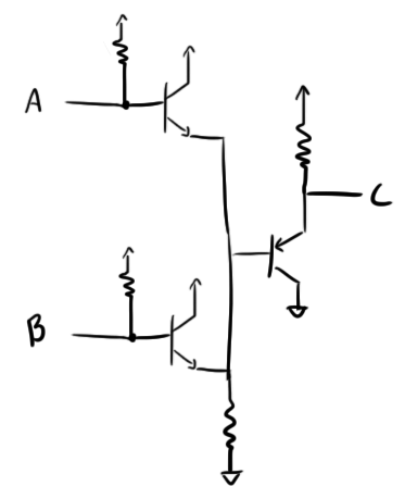
OR is a little more complicated:
In this circuit, if A is high, it will turn on its transistor and pass current down through the pull-down resistor to ground. This current will raise the voltage acros that resistor raising the base voltage of C’s transistor. This will turn it off and cause C to be pulled high. The same will happen if B is high.
When I first saw this, I thought it was a bit odd that NPN transistors were being used on the high side and PNPs on the low side. Typically, they are used the other way around. See, the issue is that BJTs only care about the current passing through their emitter which depends on the base and emitter voltages.
When you place a load between the emitter of an NPN and ground for instance, you can’t necessarily tell what the emitter voltage is as it will depend on the type of load and how much current is passing through the load (some of this current may be from other sources).
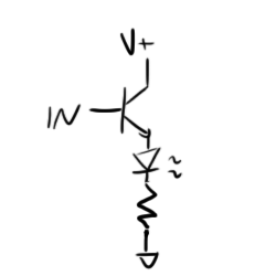
In some BJT applications like lighting LEDs this can be a real issue as you can’t turn on the BJT entirely.
In this case for example “IN” has to be .7V higher than the anode of the LED in order to allow curent to flow through the transistor. Unfortunately, as current flows, the voltage drop across the resistor will increase and the base-emitter voltage will drop below .7V again turning the transistor off. This will set up a feedback loop that will settle with the emitter .7V lower than the base and current just trickling through the LED. It probably won’t even be enough current to turn the LED on, so typically, the NPN transistor is moved below the resistor so that the “IN” signal needs only be .7V above ground to turn on the transistor entirely.
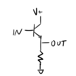
Obviously, you don’t want to severly limit the amount of current you’re passing through an LED, but what if the goal actually was to limit the amount of current drawn? Let’s say that we’re not powering an LED and only really care about the emitter voltage of the transistor:
This is a perfectly valid configuration for data signals and will allow for a very small current draw. When you’re working with tons of transistors in a circuit that is supposed to be running continuously for months, lowering current draw can lower your power consumption and make for a more efficient device.
The downside of this setup is that the output voltage will always be .7V lower than the input. This means that if the input voltage swing is from 0V to V+, the output will be 0V to V+-minus-.7V. This could be a problem if you had a bunch of these kind of circuits chained together. If you connected this OUT to the IN of a similar circuit and the output of that circuit into the input of yet another, you would end up chopping off .7V every iteration until your signal level got too close to ground to be useful.
This turns out not to be a problem because this circuit switches off between NPN and PNP configurations. In a PNP configuration, the output range is .7V to V+. This serves to “reset” the signal range and prevent any issues.
Furthermore, the circuit uses 9V logic which is very high for a data signal. It would take a lot to reduce the signal level to something unuseable.
If you’re interested, this topology is sometimes called an emitter-follower.
Conclusion
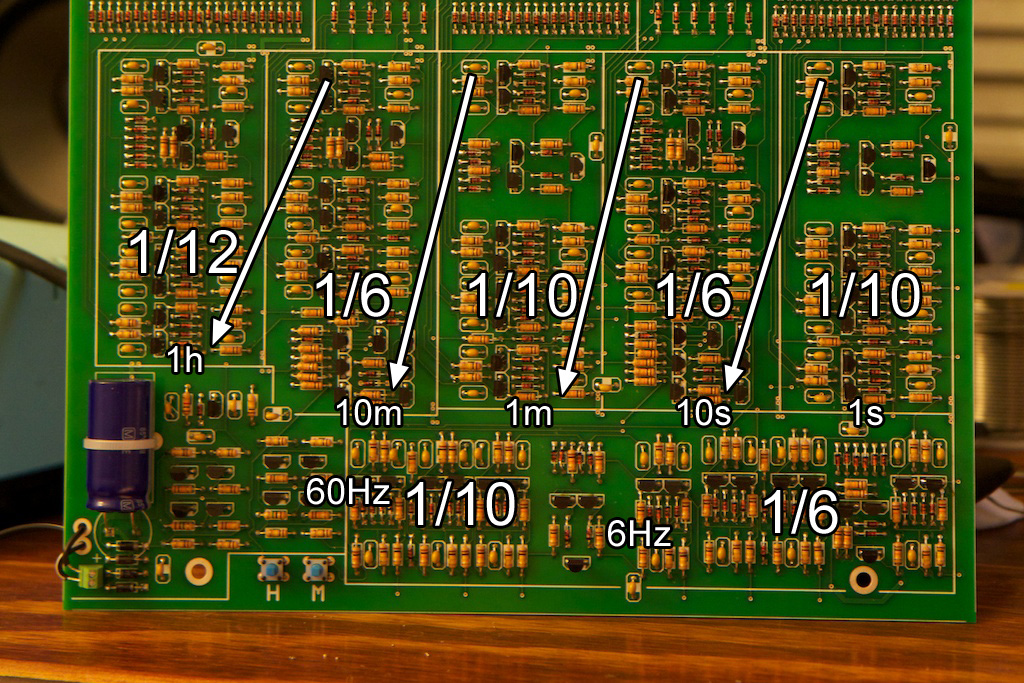
Here’s the clock with all the scalers labeled. Note that the minute->hour scalers have the same topology used in the 60Hz->1Hz scaler.
More on the 1/12 divider later.
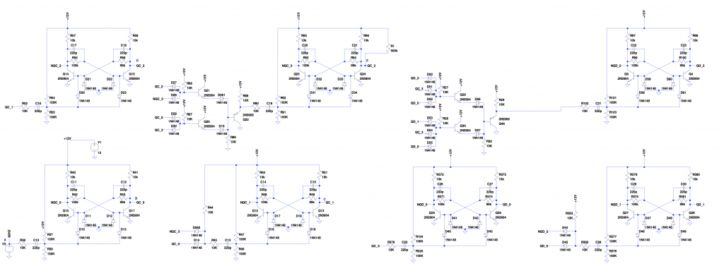
With all the gates in place, you get this:
The LTSpice model can be downloaded here.
Signals A-E from the 1/10 prescaler section are labled for your convenience. Note that the “QC” signals correspond to the 1/10 divider while the “QD” signals correspond to the 1/6 divider. I left the three-input AND gates intact with the third input signal disconnected. If you’d like to experiment around with these signals and try to figure out what they’re used for, just connect QC_3 appropriately.
So that’s all for now. Again, if you’d like to follow along at home, pick up your own transistor clock kit and grab your soldering iron!
Continue the story here.












Pingback: Transistor Clock Part 1: Power and Time Base | ch00ftech Industries
Pingback: Transistor Clock Part 3: Binary Counter and 7-segment Decoder | ch00ftech Industries
Your picture with the divisors is in error. the upper blocks are
div12(hours), div 6(tens-of-minutes), div10(minutes),div6(tens-of-minutes),div10(minuteS).
The lower two in the prescaler are correct.
This site is amazing, great job.
And suddenly I’m acutely aware of the diagram on page 25 of the assembly manual. I’ve updated the diagram to be more clear/accurate.
Thanks for taking the time to look through my work and point that out. Did you ever figure out what those extra diodes were for?
Pingback: Soil Moisture Sensor | ch00ftech Industries
Regarding the toggle-flipflop:
Your explanation confirmed my assumption of how this works. At first glance It looks really simple until it starts messing up your brain. It’s so amazing how much though you can and have to put it such simple looking schematics!
After days of searching, this is the discrete T Flip Flop I could get working, really wish it showed up in google searches.
Genial, la teoría y su forma de explicar, tienes mi respeto:) , Gracias