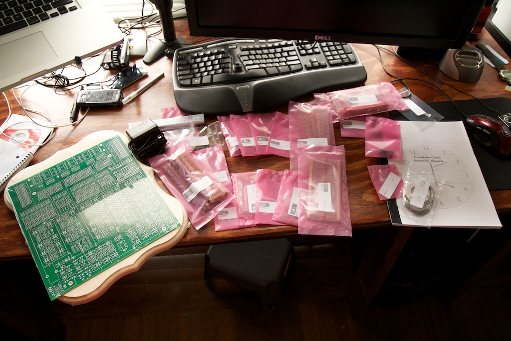
So, if you have been following me on twitter, you might have noticed this tweet where I raved about a “Transistor Clock” kit that lets you build a wall clock using 194 discrete transistors and hundreds of other components. I’ve since purchased the kit and decided to blog my assembly of it.
Exciting!
Motivation
As electronics kits like Arduino become more and more popular, the relevance of old-fashioned analog electronics is waning. There are still a lot of common problems that can be solved simply with a few capacitors, resistors, and transistors, but many people opt to use more complex (and expensive) digital systems instead.
I too have fallen victim to this trend and I feel like my analog prowess is not what it could be. I’ve had a lot of difficulty over the years understanding complex analog systems and even more difficulty trying to design them. That’s why I was excited when I saw this ad in the back of Nuts and Volts magazine:
It’s a clock made entirely out of analog components!
I’ve made a few clocks over the years (that predate this blog) such as my nixie-tube clock:
And my “Bulb-dial clock” where the hands are shadows:
As an engineer, I have sort of a thing for clocks. See, a clock is one of the few engineering problems that has been COMPLETELY SOLVED. Seriously. You can go to Wal-mart and buy a digital wristwatch that will last for years off its internal battery, travel 100 meters underwater, keep time to the millisecond, and cost less than a night at the movies. Clocks are done.
Because of this, any newly designed clock is going to be more of an artistic expression or a self-imposed engineering challenge (can we make a clock that runs off of a potato!?). The transistor clock is both.
This clock is presents a statement that in the era of integrated circuits, it’s still possible to make a clock using parts from the 1950s. Every digital circuit you build with today is abstracted out of analog components, so there is a lot to learn from working with these components directly. Perhaps the fortune cookie from my lunch could summarize:
Not really sure what they were going for there….is that supposed to be a metaphor or something?
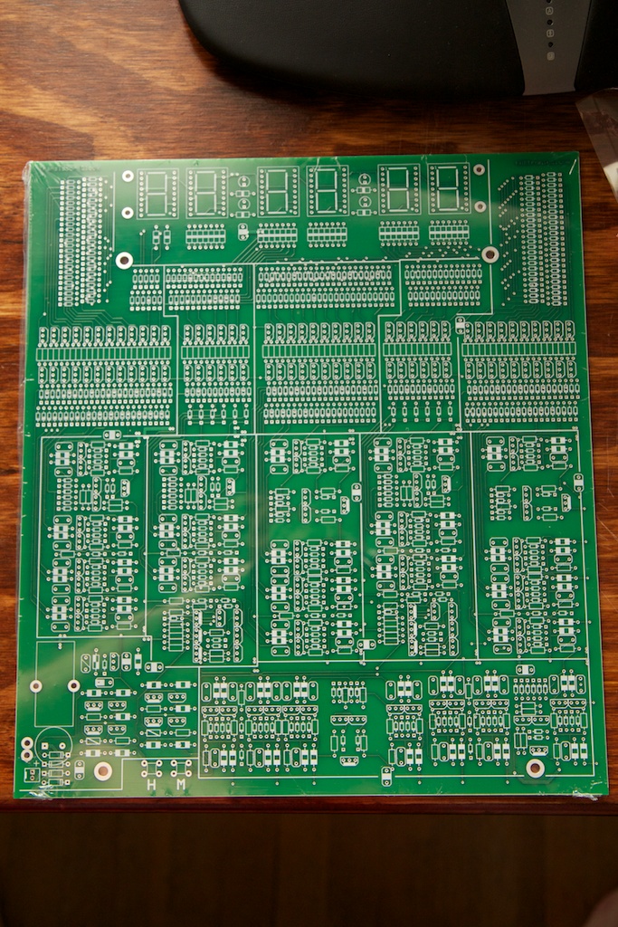
This analog/discrete-only limitation makes it hard though. One of the major gains that the integrated circuit offers humanity is the ability to pack multiple transistors, resistors, capacitors, and diodes on the same tiny piece of silicon. When you separate them, they take up a lot more space. Look at the circuit board for this monster:
That’s a lot of soldering.
It’s exciting though to have all of the components out in the open like that. There will be no “black boxes”. Every single signal path can be probed and completely understood. Cool! What an excellent learning opportunity!
The kit was mentioned on Hack-a-day where apparently the coolness of the clock is lost on the readers:
I really hope that was a troll…
The Kit
So this guy sells these clocks as kits through his website that you can assemble yourself. He sells a bunch of different versions including a nixie tube version which is extra retro.
I thought these kits were really cool, and I really wanted to incorporate one into my blog somehow, but unfortunately they’ve already been designed! I usually make a point of making things that are challenging and have never been done before, but this clock is neither (especially when you consider that it’s a kit with everything you need in the box).
I decided to purchase a kit anyway and give it the “ch00ftech treatment”. The kit comes with an assembly manual which does a pretty good job of explaining how it works, but I decided it would be fun to take it all a step further and to create a few of my amazingly long writeups that you all have come to love. I really wanted to flesh out every detail.
This transistor clock is an excellent project for hobbyists. The kit is beautifully laid out and it comes with everything you will need (including solder!) to assemble it (bring your own soldering iron though). Given how well organized it is, you don’t really even need any background in EE to assemble it. The assembly manual even has instructions on how to solder if you aren’t comfortable with soldering yet and tips for debugging issues. If you simply follow the instructions and place the components in the right holes, you’ll end up with an awesome transistor clock of your own!
If you’d like to know how all of it works though, keep reading. Over the next few blog posts, I will be discussing the different stages of the clock in detail.
Power
The transistor clock is powered by a normal-looking wall-wart transformer, but unlike a typical wall-wart, it outputs AC instead of DC. The reasoning behind this will be clear a little later.
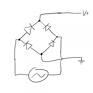
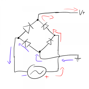
The kit comes with a 9V AC wall adapter, but the kit itself runs off of 9V DC. To create this DC voltage, we need to rectify the AC voltage coming out of the adapter. This can be accomplished using a “full-wave bridge rectifier“. This circuit is actually inside a lot of cheap DC wall-warts anyway:
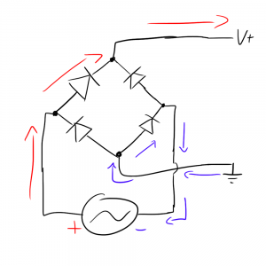
The idea is that no matter what polarity the AC input has, current flowing out of it can only flow in the desired DC direction i.e. charge flows out through the V+ connection and back through the ground connection:
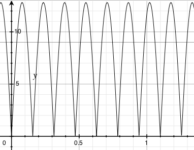
This presents a few problems. As you can imagine, there will be points in the cycle where the AC potential is at a zero crossing where no current will flow into or out of it. In addition, you have to remember that the AC voltage is measured in Vrms, so the peak voltage of the 9V adapter that the kit comes with will actually be around 12.8V which is much higher than the desired DC output voltage of 9V. The waveform might look something like this:
Where the horizontal line is at the target 9V mark. Note that the area under the waveform is equal to the area under the 9V line.
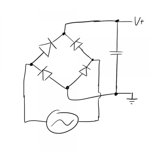
To solve this problem, a large output capacitor is placed across the DC rails. When the AC voltage shoots above 9V, the excess charge will be stored in the capacitor, and when it drops to zero, the charge in the capacitor will power the circuit. Essentially, the capacitor acts as a simple low pass filter that should keep the output voltage fairly stable.
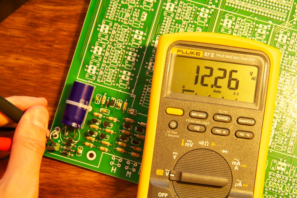
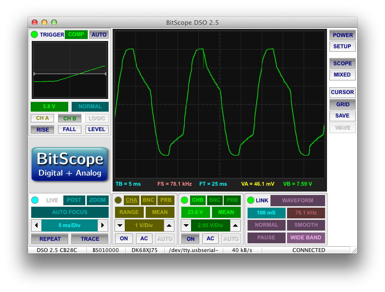
I quickly assembled this part of the circuit and ran some tests on it. Here’s the AC voltage out of the wall adapter:
And the rectified DC voltage with a 470
![]()
load:
Huh…well that doesn’t seem right. So first of all, there is very little load on this circuit, so it makes sense that the DC voltage is higher than the AC voltage. Basically, there isn’t enough load to pull the excess charge out of the output capacitor, so you end up with your DC voltage being closer to your peak AC voltage.
As far as the AC voltage is concerned, it is kind of weird that my 9V adapter is putting out 12+ volts.
Update:
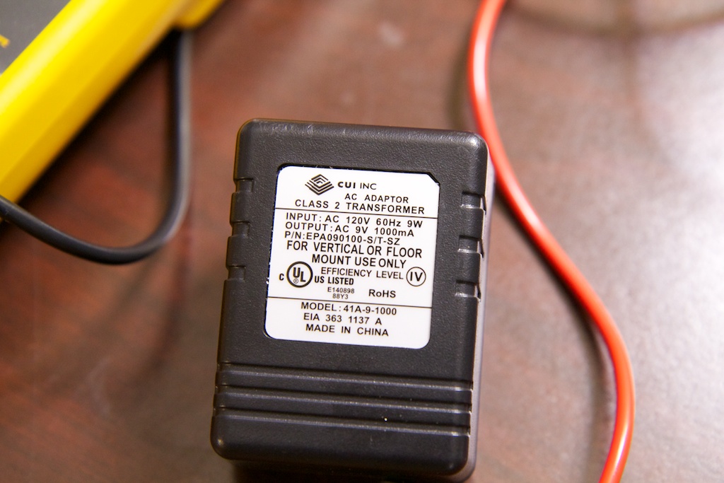
I had a little time to investigate the issue of the AC adapter output. Turns out that this is a result of the AC adapter being entirely unregulated. Looking at the adapter, you can see that it’s rated for 9V at 1000mA.
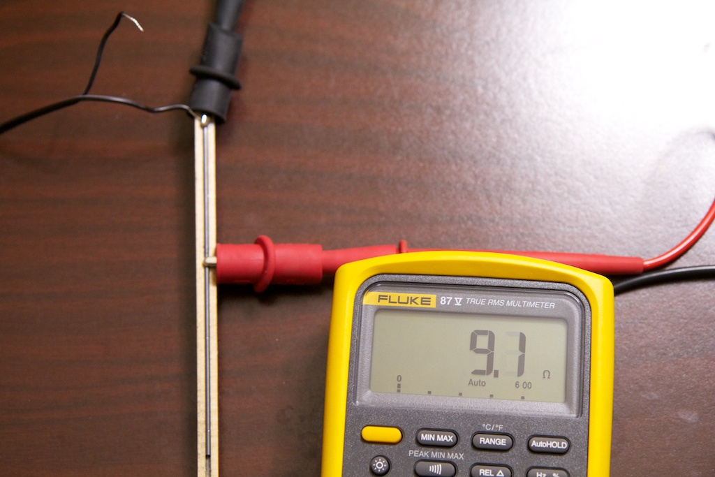
This rating takes into account resistive losses that the adapter may have on its windings. I measured about 1.9
![]()
on the secondary winding and over 200
![]()
on the primary. When outputting 1000mA of current, these resistive losses inside the transformer will drop the output down to the proper 9Vrms. To test this, I made a 9
![]()
power resistor out of pencil and put it to the test.
As you can see, with a 9
![]()
load, the power supply is outputting 1000mA of current and its output voltage drops to a proper 9Vrms. Resistive losses in a transformer are unavoidable. Typically, more sophisticated switching power supplies compensate by adjusting their duty cycle or passing the output through a linear regulator. Because this is not a sophisticated power supply, the designer chose to solve the problem by simply changing the winding ratio so that the open-circuit voltage was much higher than the target load voltage.
One of the benefits of a completely analog system is that it’s very tolerant of poor voltage regulation (i.e. won’t blow up if the power supply shoots up by 10-20% or so).
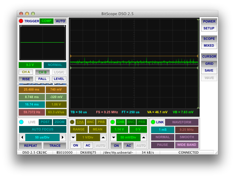
The important thing is that I’m getting a DC output. I hooked my oscilloscope up to the DC voltage rail and put it in AC mode. This would take away the DC component of the output and let me measure the voltage ripple:
As you can see, there’s less than a volt of ripple which is acceptable.
Time
One of the first questions you might have when presented with the idea of a completely analog clock is “What does the clock use for a time base?”. This was definitely my first question. Most analog circuits use components like the 555 timer to generate clock signals. The 555 depends on RC time constants to generate the frequency. Unfortunately, resistors are usually sold at 5% tolerance values and capacitors at 10-20% tolerance, so it’s difficult to create a perfect clock. Even if you could (perhaps with a trim potentiometer instead of a fixed resistor), resistor and capacitor values can change slightly with temperature variations, and your clock would definitely become inaccurate over time.
Reading into it, I found that the transistor clock actually uses the 60Hz in a wall socket to keep time. This might come as a surprise as usually time is kept accurately with something like a crystal oscillator, but apparently a lot of clocks have come to depend on the precision of the 60Hz AC signal coming out of the wall. These are called “Synchronous Clocks“. These clocks are pretty accurate. In fact, power providers will often change their frequencies during off peak hours to compensate for any drifting during high-use hours.
In a later post, I will be putting my AC line to the test and comparing it to a crystal oscillator.
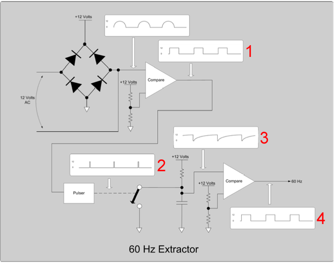
The goal of this part of the circuit is to take the 60Hz sine wave coming in and somehow convert it to a 60Hz square wave output. Here’s a block diagram of how it works taken from page 30 of the assembly manual which I have marked up a bit:
Although the circuit itself runs off a 9V power supply, all of the explanation pages in the assembly manual are drafted with a 12V supply. The circuit’s performance should be relatively unaffected by this, so I will be using 12V as well in my explanation to keep consistency with the manual. Note that my actual oscilloscope traces will be on a 9V circuit.
I will be explaining the four stages in the following paragraphs. Keep in mind that I will be using an LTSpice model to demonstrate the stages in action. LTSpice is a free application that is great for simulating analog circuits. There is a link to download this model at the bottom of the page.
1. Comparator
So the first part of the signal path simply compares part of the AC waveform to a fixed reference voltage. The idea is that every time the AC waveform is at a higher potential than the reference voltage, the output will go high. Otherwise, the output will be low. This will generate a square wave that will have the same frequency as the AC waveform:
The AC waveform is tapped off of the diode-bridge. Because the AC supply is not tied directly to any part of the DC rails, it will tend to float. This means that when you measure part of the AC supply referenced to the DC ground rail (as you might do with an oscilloscope or multimeter), you might not get a perfect sine wave. The author of the above block diagram showed this waveform as a sine wave passed through a half-wave rectifier:
Which is basically all the positive parts of an AC waveform.
I didn’t see this waveform on my LTSpice model or my actual circuit. I saw something that looked more or less like a sine wave:
It doesn’t really matter. The important thing is that it’s a waveform that crosses the reference voltage twice per cycle.
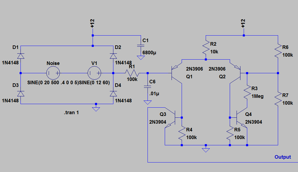
Here’s a schematic of the whole first stage:
A few small comments before moving on to the comparator:
- You will notice two voltage sources in series. The purpose of the “Noise” source is to introduce a blip of noise into the AC line to see how well the circuit responds to this noise without losing time. In reality, a similar blip might occur whenever you switch on a high power device (hairdryer) that is connected to the same circuit breaker as the clock.
- R1 and C6 serve as a simple low-pass filter with a cutoff of 160Hz. Because the circuit only needs the 60Hz fundamental frequency, this filter will help cut out unwanted noise that could negatively affect the clock.
- R6 and R7 create a voltage divider that provides a DC reference voltage of 6V into the comparator.
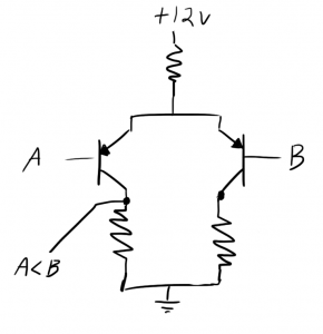
A simple analog comparator or “differential amplifier” might look something like this:
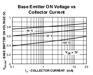
The principle behind how this comparator operates is based on the ON voltage of a BJT. Most PNP BJTs “turn on” when their emitter-base voltage is .7V or higher. You can see this in the 2N3906 datasheet:
Where the emitter-base voltage is around .7V at room temperature. When a BJT turns on, it draws a large amount of current from emitter to collector. Let’s look at the example of a single BJT in a similar configuration:
As soon as the base voltage drops more than .7V below the emitter voltage, current will start to flow through the resistor. Due to Ohm’s law, this will cause a voltage drop to form across the resistor lowering the emitter voltage. If the emitter voltage drops to within .7V of the base, the transistor will turn off and the emitter voltage will start to rise again. Of course, the rising emitter voltage will turn the transistor back on causing it to drop again. This feedback system will keep the emitter-base voltage at .7V.
In addition to this, the emitter-base junction of a PNP transistor looks like a standard silicon diode with a .7V-ish forward voltage. Even if the collector wasn’t connected to anything, this diode would maintain the .7V emitter-base voltage.
Now imagine two of these transistors configured as in the previous schematic. Neither BJT can maintain an emitter-base voltage greater than .7V. Because of this, the emitter voltage that they share will drop down to .7V higher than whichever signal (A or B) is at the lower potential.
For example, if A is at 5V and B is at 6V, the common emitter node will drop to 5.7V. Because the emitter of B will then be .3V lower than the base, B will turn off entirely. In this configuration, the “A<B” terminal will rise because of the collector current passing through the low side resistor. In effect, the “A<B” terminal goes high when A is less than B. Go figure.
Now, there is a pretty serious problem with this configuration. The collector voltages of each BJT are allowed to float all the way up to the emitter voltage. This means that even though the emitter-base voltage might be high enough to turn the transistor on, current still won’t flow because the emitter-collector voltage isn’t high enough. As a result, the output voltage might get stuck in some indeterminate state if A gets too close to B.
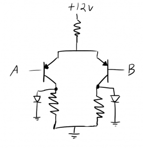
There needs to be a way to limit exactly how high the collector voltages can get. This can be accomplished easily using two silicon diodes:
These diodes will not pass any current until their BJT’s collector voltage reaches their forward voltage (around .7V). At this point, they will conduct and keep the collector voltage at .7V. This guarantees a steady flow of current out of the collector as soon as the transistor turns on.
This presents another problem though. If we were to read the voltage at the same point we were before (our “A<B” signal), the output signal will be a square wave between 0 and .7V. This isn’t a very useful voltage range.
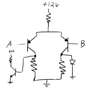
This problem can be solved by replacing one of the diodes with the base-emitter junction of an NPN BJT. By itself, this junction will look like a standard silicon diode with a forward voltage of .7V. It will also have the bonus effect of pulling a lot of current through the collector when turned on. When connected to a pull up resistor, this acts as a signal amplifier.
This will also invert the signal so when A is greater than B, the output will be high.
Now this is a perfectly fine comparator circuit, but it does have some room for improvement. One of the biggest problems with comparing two signal is noise. A little noise on a singal line can cause multiple output transitions to occur when only one is expected. Consider this drawing:
From far away, you might only be expecting a single transition, but as you can see closer up there are actually more. This can be problematic for something like a clock. It might count two pulses where there is only supposed to be one causing it to count too fast and lose accuracy.
There are a number of solutions to this type of problem perhaps the most common being a “Schmitt Trigger” input. The idea is to basically force the signal to commit to one output or the other and to not let it sit on the fence. This principle is sometimes called “hysteresis”.
In our circuit, one solution is a simple positive feedback system. Basically, as soon as the sine wave passes higher than the reference voltage, we will lower the reference voltage slightly. This means that in order to skip back, the noise on the sine wave must be great enough to drop the signal below the new lower reference voltage.
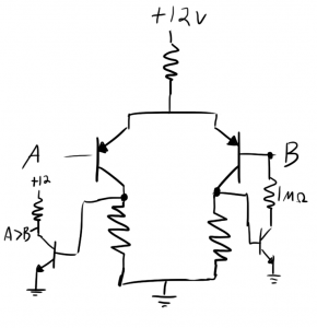
This positive feedback system is created using another NPN transistor that pulls down on the reference voltage (B) lightly:
Note: At this point, the two low-side resistors aren’t exactly necessary, but they’re still a good idea due to the frequency of this circuit. Without them, the A and B transistors will take longer to shut off. Those resistors quickly pull the bases to ground.
As soon as A rises above B, the B-side PNP transistor will turn on which will turn on the B-side NPN transistor pulling B down slightly. When A dips below B, this all returns to its previous state, and B rises slightly. It’s a simple addition that will help reduce the number of mis-counts even when a lot of noise gets introduced on your AC line (someone runs the blender and microwave at the same time).
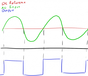
You can see this happening in the following waveform trace from LTSpice where red is the AC input signal, green is the DC reference voltage, and blue is the output.
Note how the reference voltage jumps up and down slightly as the AC waveform crosses it.
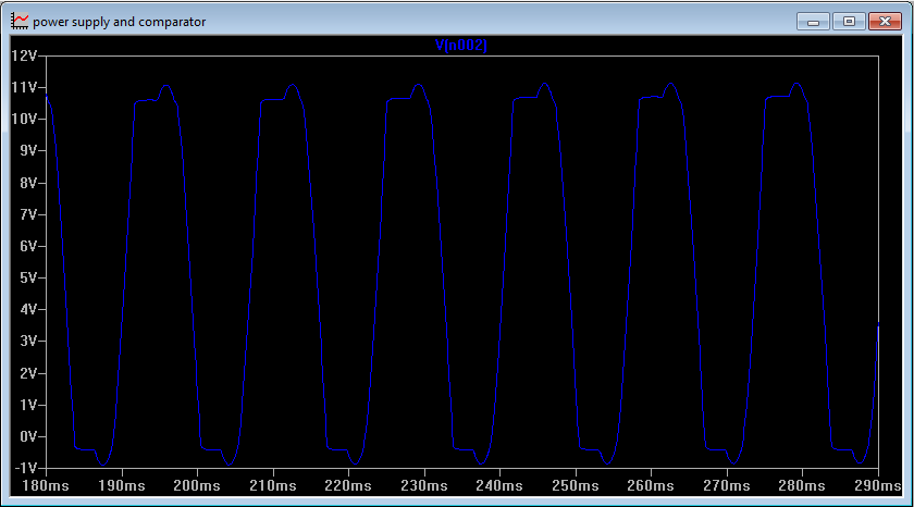
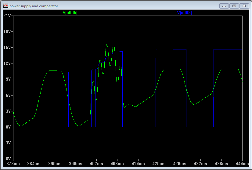
Alright, so now we have an output square wave. We could stop here, but there is still some room for improvement. To demonstrate a potential issue, I set the “Noise” source to emit a high frequency pulse for a brief period of time to see how it would affect the output square wave. Here you can see the input wave in green and the output square wave in blue.
It looks like this noise was still too much for our hysteresis solution above and the output square wave looks like it blipped low for a brief moment. If we were using this blue wave as our clock, this would cause it to suddenly jump 1/60th of a second ahead. A lot of these blips could cause the clock to slowly drift ahead of real time.
So how do we solve this? The solution is to create a “pulser”
2-4: Pulser and comparator
The goal of the rest of the circuit is to create a low-pass filter of sorts. Instead of being applied to an analog signal, it’s applied to a digital signal. We want to make sure that any blips that are too close to a previous clock transition are ignored. We will essentially be using an RC time constant to measure the time between low to high transistions on the square wave and make sure that they are far enough apart.
These next three stages work very tightly with each other. It’s not easy to dive into the circuit specifics without first understanding the overall goal. The next few paragraphs should provide an overview of the goal which I will follow with the circuit specifics.
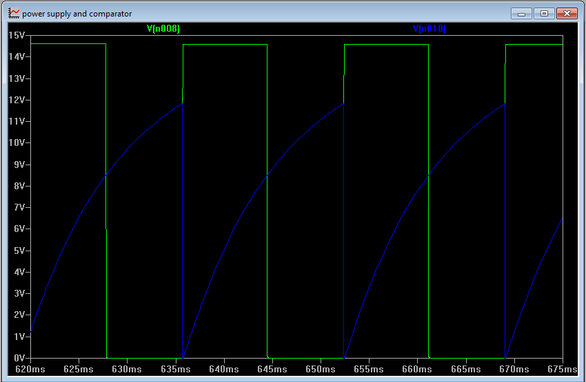
The idea is to completely discharge a capacitor every time the clock pulse goes high and then begin charging it through a resistor. This slowly rising capacitor voltage will be fed into another comparator with another reference voltage which will produce another square wave output.
Here you can see the input square wave (coming out of the first comparator stage) in green and the resulting capacitor voltage in blue. Note how the capacitor voltage drops to zero every time the input wave goes high:
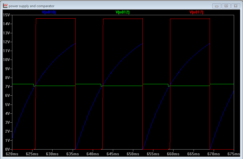
And here is that capacitor voltage again along with the second reference voltage in green and the new output square wave in red:
To see how this can help reduce noise, take a look at the following waveform:
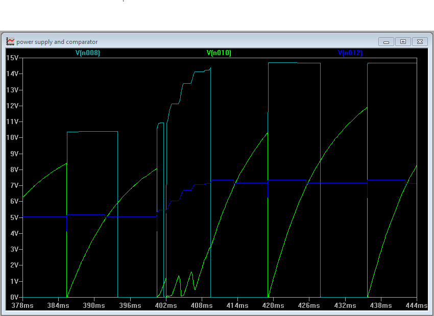
Here you can see the output of our first comparator in teal along with the capacitor voltage in green and the second reference voltage in blue. Although the first comparator’s output has a spurious pulse due to noise, the capacitor voltage crosses the reference voltage the same number of times as it would have if there was no pulse. This has effectively rejected the signal noise and kept time accurate.
Now how the hell do we do this?
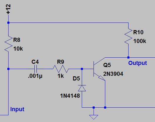
The first challenge is to create a circuit that will discharge the capacitor only on low-high transitions. This is called a “pulser”.
A note:
- R8 is the pull up resistor from the output of the previous comparator
While the input is low, the voltage across C4 will be zero. As soon as the input rises, the voltage across C4 will start to rise, and current will begin to flow through C4 and down to ground through Q5. This will turn on Q5 and pull the output low.
This current will not last long though. Remember the formula:
![]()
The current through C4 is proportional to the rate of change of voltage across it. While the voltage is rising, current will flow, but once the voltage stops changing, the current stops as well. This means that Q5 will turn off and the output will rise again.
The same will happen as the input voltage drops, but the current will flow the other direction out of D5. Without D5, the base of Q5 could be stuck at some negative voltage and wouldn’t make it back to zero for the next cycle.
The end result is an output pulse that shoots low only while the input voltage is rising. If this output was connected to a capacitor, you should see the expected waveform where the capacitor discharges quickly through Q5, but rises slowly using the current from R10. It is assumed here that the collector current through Q5 is high enough to discharge the capacitor completely in the short period of time during the pulse.
Sizing that capacitor properly is important. If the capacitor is too small, it won’t filter out undesired pulses. Make it too large, and you might end up filtering out the clock itself. Because noise is unpredicatable, there is no way to find an optimal capacitor value. You can find an upper bound on it though. Because the capacitor voltage is being compared to a threshold that is half of the rail voltage, you can say that it will take slightly less than one time constant for the capacitor voltage to reach the threshold (1 time constant is around 64% of the final value)
This means that the product of R10’s value and the output capacitor’s value cannot be more than 1/60 seconds. Any longer and you would filter out desired clock transitions. If R10 is set at 100k
![]()
, the capacitor should be:
![]()
So the value must be less than .16
![]()
F. The kit’s designer chose .1
![]()
F which is an appropriate value.
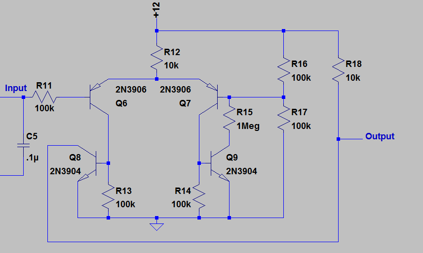
So that’s basically all that’s new. The only next step is that output capacitor (C5) and another comparator just like the first one:
Conclusion
Putting all of this together, we get this:
The LTSpice model for this circuit can be downloaded here.
So there you have it folks. This circuit will take the signal coming out of a 9V AC transformer and produce a 60Hz square wave that can be used to run a clock.
Although I haven’t read too far ahead in this manual, I think this stage of the clock has the largest variety of concepts. Most of the rest of the clock is highly repetitive, so large sections can be explained in a short period of time.
If anything was unclear, I recommend downloading the LTSpice model and poking around at the circuit. Or you can buy your own transistor clock kit and play with the real thing!
Continue the story here.










Awesome writeup, it’s great you take the time to explain these things in such detail, thanks! I look forward to the next bit
You bought a kit.
You are enthusiastic about this kit.
The instruction manual for the kit explains the synchronous clock, the edge triggered T flipflop, and the diode ANDgate / ORgate used in the kit. But you want to reword the explanations and convert some of their glory into your glory.
Why?
Aren’t blogreaders intelligent enough to understand the original kit explanations and the original kit .pdf files, all by themselves? Why do they need you?
What is your “value added?”
I’m not trying to steal any glory from anyone.
If you read the manual for the kit, it includes a circuit schematic along with a rudimentary explanation of each of the sections. My “value added” is a more in-depth discussion of each of the subcircuits making up the clock. For example, if you look at page 34 of the manual, you will see a simple two paragraph description of a comparator. I consider myself intelligent, but I personally needed a bit of time to understand exactly what was happening in the circuit. For example, the manual doesn’t explain the need for diodes (or BJTs) off the collectors. Also, it only explains how the circuit works, but doesn’t really give any insight as to why it was designed the way it was. I thought I would expand upon that explanation on my own blog for the benefit of anyone starting out.
I know this is an unusual post considering my blog’s history; I struggled a lot with finding a way to create my own “glory” as you put it. When it came down to it, it was something I wanted to make, and it wouldn’t really add anything for me to try to duplicate the circuit. It definitely wouldn’t make sense for me to try to make my own circuit board, so I decided to just build it from a kit and write about it. I also added scope traces and a downloadable LTSpice model that was not included in the kit.
Besides, part of the reason I write this blog is to make sure that my understanding of a topic is not only thorough enough for me, but also thorough enough to explain it to others. In effect, I’m learning better by explaining, and I plan to refer back to this post when I come across similar circuits in the future.
What makes you think this blog post is even intended for your personal benefit? Very little of the theory he’s covered here is anything that is not beaten to death in the first year or so of directed EE studies. By your metric, the only “value added” in this blog is the occasional novel aspect of his designs.
The best way to learn is to teach, and that is pretty obviously the focus of ch00f’s writing. Having gained a little knowledge and a lot of inspiration here, I have a lot of respect for that fact (and for him).
If your knowledge is so advanced that you gained literally nothing from reading this post, perhaps you should be writing your own in-depth designs and analyses and share that mountain of wisdom – and enjoy the benefits of random internet morons claiming that you bring nothing to the table.
Thanks for your support, but there’s no reason to call anyone names.
My jimmies, they are rustled.
On top of that, some of his explanations are not very good and simplify things so much that how they actually works is lost.
Pingback: Transistor Clock Part 2: Prescaler | ch00ftech Industries
Neat kit; but I suppose this wouldn’t work too well in the 60Hz side of the world 🙁
A discrete frequency synthesizer to multiply the signal by 1.2? Shudder..
What do you mean? It works perfectly well in the 60Hz side of the world!
Check out part two:
https://ch00ftech.com/2012/07/10/transistor-clock-part-2-prescaler/
Building a 1/60 frequency divider is tough, but you have to do it anyway if you want 60 seconds in a minute and 60 minutes in an hour.
Pingback: Transistor Clock Part 3: Binary Counter and 7-segment Decoder | ch00ftech Industries
Pingback: Are you sure about that 60Hz? | ch00ftech Industries
Wonderfully detailed, ty for taking the time to do this! Q: tried to find a link to the bulb-dial project, no luck. Can you show me where on the blog that is, pls? Also: do you still have parts list &/or circuitboard for that? Thx either way! 🙂 (feel free to email me rather than post this if you’d prefer.)
Thanks! The Bulb-Dial clock actually predates my blog by a few years. I didn’t document any of the process, and I don’t think I even have a parts list or even the source code for it. Sorry!
Pingback: QR Clock | ch00ftech Industries
Pingback: Bringing a Car Battery Back from the Dead: A Ch00ftech Halloween Tale | ch00ftech Industries
Hi!
Wandering through the Net, I just found your blog. Kudos for packing it with such detailed explanations and good photography. I really like it!
There is a small issue however in one of your sentences. You wrote: “Note that the area under the waveform is equal to the area under the 9V line.”
Actually, if 9 V is the RMS voltage, then the area under the waveform should be somewhat less than that. That’s because the RMS voltage of a sine is peak/√2, whereas the average rectified voltage is 2×peak/π, ignoring the diode thresholds. That’s about 10% below RMS.
Regards,
Edgar.
You are absolutely correct. While the average power delivered to a load by each waveform will be equal, the average voltage will not. It looks like I mixed those concepts up while writing. Good eye and thanks for the correction!
Pingback: Electronic Birthday Candle | ch00ftech Industries
Well put!
I gained a lot from this blog post, the scope traces were a great learning aid too.
Great write up and really drove home some concepts for me. Don’t let the trolls win. Keep writing stuff like this and people like me will keep reading … And posting our own projects.
Well donne !
you are amazing that what i am calling the new design
your project is very helpful for me and it is very sample to undertand
i love the circuit that using transistor only !
keep dong this project, i love this plog
Howstuffworks.com has a much simplified version of this project. However, I believe their instructions for generating a clock signal are wrong.
After transforming to the appropriate voltage, they say to take 60 hz wall power and pass it through a bridge rectifier. One terminal is then hooked to a resistor, and a zener diode is hooker from this resistor to ground. A wire from the zener and resistor is supposed to supply a 60 hz clipped wave.
However, given that a bridge rectifier is full-wave and not half-wave, wouldn’t this clock signal actually be 120 hz?
(I built the circuit exactly as given and my clock is twice as fast as it should be.)
That sounds right. Strange that they told you to do it that way. Maybe they forgot to mention a clock divider somewhere?
Hello,
Thank you so much for that article. Compared to a lot of material on the Internet, you explain WHY this and that component is here: this is great. Most (of those i happened to visit on my Google trip) just use simplified circuit or do not bother with more than “the capacitor pulls the charges from the base”.
To react to the negative comment, I am an engineer (so reasonably intelligent I guess) but never specialised in EE. Looking into circuits as a hobbyist, this sort of explanation is exactly the thing to recall and piece together what I learned at school
I realize the question is a bit off topic here. I started learning the ropes of electronics just a few weeks ago and my question may sound stupid for a pro like you, but I’m still going to test my luck and – hopefully – somebody here will help me out. Thin is, I’ve been trying to figure out the difference between a bridge rectifier and a rheostat. When it comes to bridge rectifiers I guess I mostly understand how it works thanks to your article and the video on this page https://www.derf.com/how-a-bridge-rectifier-works-step-by-step-tutorial/ , but it’s more complicated with rheostats for me. What’s the biggest conceptual difference between the two? Thanks