It’s funny how sometimes the simplest projects can give you the most trouble.
Background
Ever since our friends at Apple decided that people don’t need to swap out the batteries in their phones, there has been an entire industry of creating external battery packs that will allow users to get more Tinder and SnapChat out of their devices when their busy lives keep them far from an outlet.
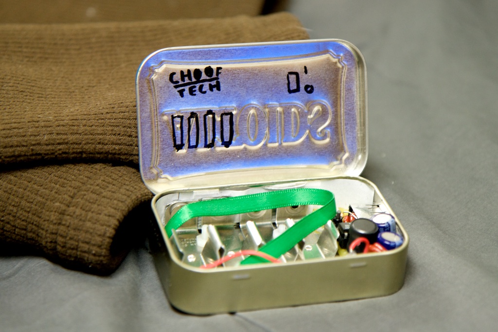
Companies like Anker and Mophie offer options that range from battery packs with multiple USB outputs and solar panels to packs built directly into phone cases. I’ve even taken a stab at this myself; in fact, the first time I ever used the name “ch00ftech,” it was hastily written in sharpie inside a Mintyboost that I made for my dad for Christmas back in 2009:
With 4 fresh AA batteries, this baby will provide enough juice to fully charge an iPhone 3Gs. That is if the battery terminals don’t short to the Altoids tin.
I also purchased a 15,000mAh Anker to shoot the video for my Gutenberg clock and have since started carrying it around every day.
With so many portable battery solutions available, you might wonder why I would bother to make yet another. About a year and a half ago, I decided to cancel my bus pass and start commuting to work via bicycle. This was partly to help me get in shape, but it was mostly because commuting the daunting one mile from my apartment to the office by waiting 15 minutes for a bus to show up was a little ridiculous.
Biking is popular in Seattle, but despite its growing amenities for cyclists, the city is still only considered the 13th most bikeable in the U.S. It would rank much higher, but no matter how many protected bike lanes you add to your roads, the hills still present a problem.
Even discounting the physical exertion required to get up these steep peaks, slowing to a snail’s pace on an incline while surrounded by cars zooming uphill can be a pretty scary scenario. Because of this and a well placed telephone pole flyer, I decided to purchase an electric assist.
Clean Republic is a Seattle-based retailer of electric bike kits. Their “Hill Topper” offers a front-hub motor, battery pack, and motor controller all for a fairly reasonable price. Because it powers the front wheel exclusively, there’s no need to worry about chains and sprockets, so installation was a snap for a sparky like me.
Most importantly, having a 24V/7Ah lithium iron phosphate battery pack opens up a lot of interesting opportunities for someone with an electronics background. One example is this safety measure I added.
I probably won’t be doing a writeup for that particular mod, but if you’re interested, it’s a 24V moped horn from Ebay, a simple FET circuit, and a pressure switch that I had originally purchased as a potential user input device for the bullet counter.
It was only a matter of time before I wanted to find a way to put that enormous battery to work, and a phone charger was the obvious result. Besides, with everyone on the West Coast bracing for the “Really Big One,” I thought it’d be nice to have a means to charge my phone if I’m without power for an extended period of time.
Battery
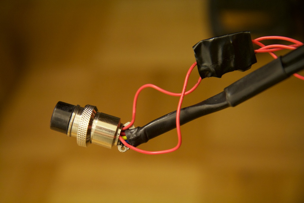
The battery pack weighs a little over five pounds and actually contains the battery cells and the motor controller. For the horn mod, I simply soldered wires into the terminals present on the bike-side of the connection:
But this time around, I wanted something that I could separate from the bike and take with me. First, I needed to figure out what kind of connector the battery used.
One of the most difficult tasks you ever may be given as an electrical engineer is identifying a particular connector. I’ve always found it hilarious in the film Blade Runner how somehow in the future, robotic snakes are manufactured with a complete part number printed on every single scale:
Yet today, you’d be hard pressed to find a manufacturer or just about anything on a part you rip out of an electronic device.
With no identifying marks present on the connector, I tried reaching out to Clean Republic, but I was told that the connectors are specified by the manufacturer of the kits. They couldn’t help me.
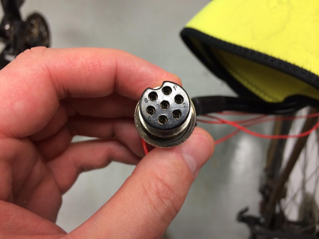
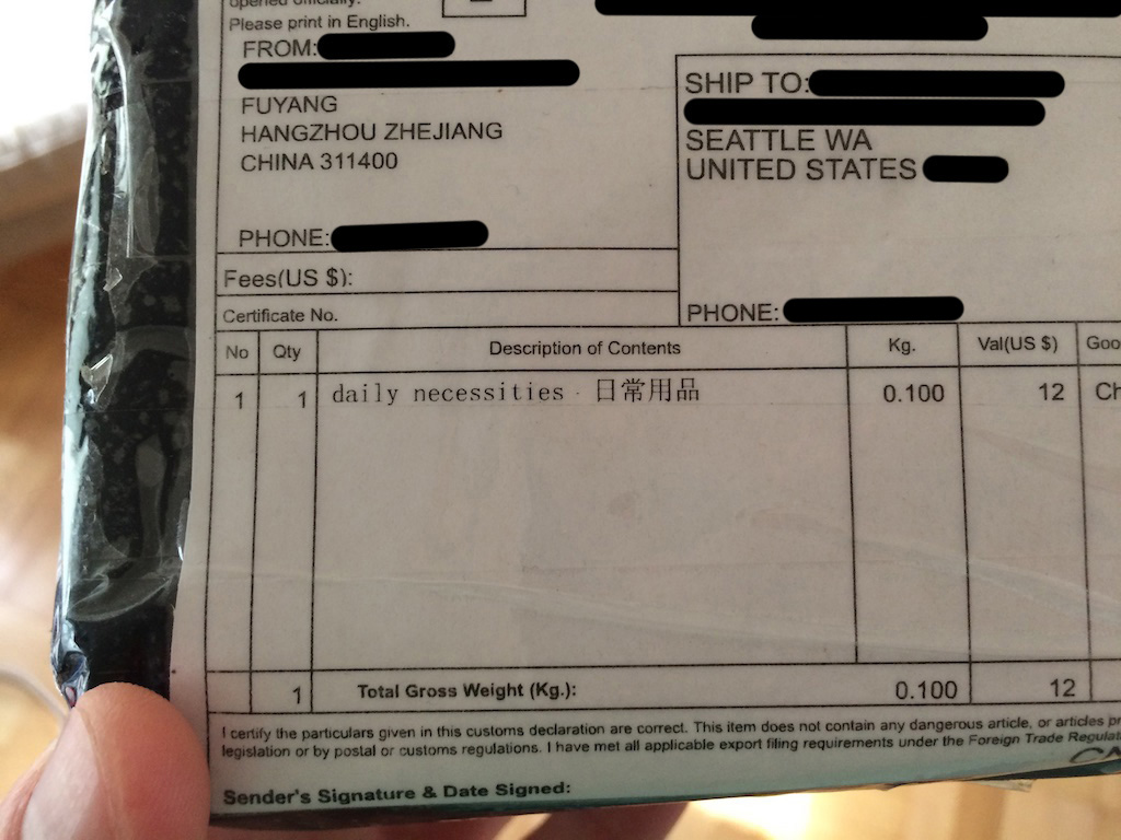
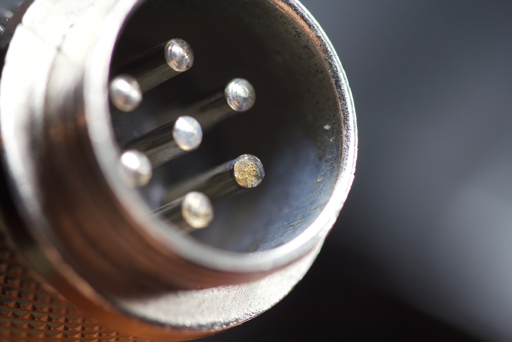
After a few hours of sifting through Google image searches to find something that looked similar and the help of a Reddit thread, I was able to identify the part as a “GX-20” connector. These waterproof connectors are apparently used in aviation applications, and they’re available on Ebay with free shipping for $12. After a few weeks of waiting, I received a male and female connector that fit perfectly.
Strangely, their packaging was labeled “Daily Necessities.” I’m wondering if that’s a way to avoid a tariff or if people in China just go through connectors really quickly.
Probing the connector on the battery, I found that Pin 1 was 26V higher than pin 6, so I used those for my power rails. I’m not sure what the other pins do. Most of them are at GND potential (maybe they’re coming from the motor driver and are GND when it’s switched off). Pin 7 (center pin) is at around 5V. My guess is it’s associated with the handlebar switch used to activate the motor.
Electrical Design
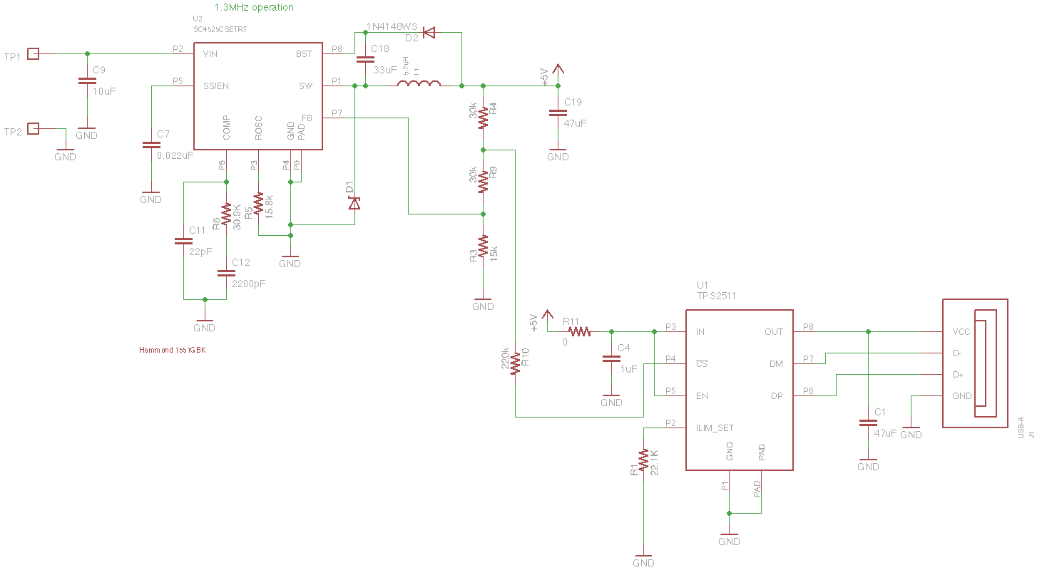
As you’ll find later in this writeup, this schematic is not the first one I tried, but I was pretty close on my first go despite all the problems I had.
USB
USB has been around for almost two decades, and during that time, its primary function has changed dramatically. What was once a simple connector for computer peripherals like mice and keyboards has become the primary power cable for a plethora of electronics including just about every smartphone and at some point in the future laptops (though the connector is different).
The problem with using USB as a power port is that the connectors have stayed the same for 19 years, but older ports can’t provide the power necessary to charge newer devices. USB has a system built into its protocol by which the downstream device (phone) can request a certain amount of power from the host device (desktop computer) which it is then either granted or denied.
This digital negotiation of course requires a host device that’s smart enough to establish a USB connection and communicate digitally. Not a problem for a laptop, but it would easily increase the cost and complexity of the cheap off-the-shelf USB chargers you find in the checkout line at Walgreens.
The official USB spec has a solution for this called “Dedicated Charge Port” or “DCP”. The spec is a pretty lengthy read, but the gist is that in addition to looking for digital communication, devices can also look for the two USB data lines to be pulled to specific voltages. These voltages indicate to the downstream device how much current it’s allowed to draw.
In order to get a phone to charge at its fastest rate, you have to set the data lines on the charger to specific voltages that indicate how much current it can provide. Of course, because nothing is easy, there are a number of other specifications outside of DCP that certain phone manufacturers choose to use, so a simple resistor divider won’t always cut it.
Fortunately, TI makes a part called the TPS2511. In addition to limiting current to the USB port for safety (if you jam a paper clip into the port), it can also scan through a number of different charger protocols to reach the widest variety of different phones.
One other neat feature is that it will pull a pin low when the output current reaches about 50% of the maximum. A number of DC/DC voltage step-up/step-down converters have adjustable voltage outputs which can be set using a feedback pin. The converter will attempt to keep this pin at a specific voltage by adjusting its output voltage. If you have the pin connected through a resistor divider, you can set the output voltage with the resistor values.
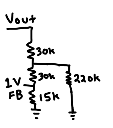
In the case of the part I was using, the feedback pin tries to stay at exactly 1V. Using the standard resistor divider formula:
![]()
![]()
Which is the standard 5V output of USB. What’s neat about the TPS2511 is that it can be set up to nudge the output voltage a little higher at higher currents. This is very useful because at higher currents, the resistive losses in the USB cable and connectors will cause the voltage at the phone to drop substantially and may cause the phone to charge slower. If a 220k resistor is inserted and connected to the TPS2511’s pin, it will boost the output voltage slightly when that pin is pulled to ground:
First you can figure out the current below the FB pin:
![]()
Which will also be the current directly above the FB pin. This tells you the voltage at the intersection of the two 30k resistors:
![]()
With that voltage, you can solve for the current through the 220k:
![]()
Finally, use the current in the two legs to solve for
![]()
:
![]()
![]()
So when the current draw gets high, the TPS2511 will boost the output voltage to 5.23V to try to overcome the voltage drop in the cable/connectors.
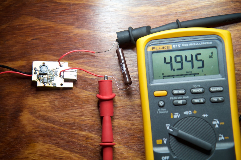
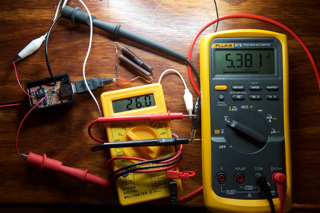
To test this out, I tried attaching a 5
![]()
power resistor to the output:
And then dropping it down to 2.5
![]()
by putting another in parallel:
Bullseye!
Buck
Now that we’ve figured out how to deliver 5V to a phone, we need to figure out how to get the 5V in the first place. When it comes to efficiently reducing voltage, a buck converter is the way to go.
For a really good explanation of how a buck converter works and how to size its associated components, you can read my writeup here.
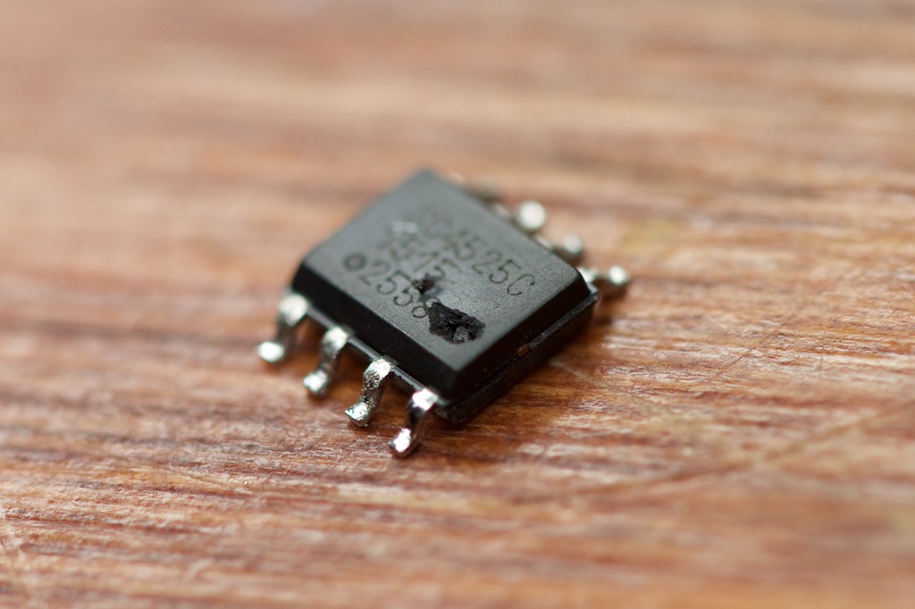
When it comes to the buck regulator, this time around I went with the Semtec SC4525C. Unlike the LM2576HVS-12 that I used in that other writeup, the Semtec part has an adjustable output and an external compensation network. Adjustable output wasn’t necessary, but I’m working on another design that will use this part, so I thought this simple project would be a good way to test it out.
Problems
Printing and stuffing the circuit went off more or less without a hitch. The TPS2511 has a fairly small pitch, but it’s not insurmountable with some solder wick to pull away shorts.
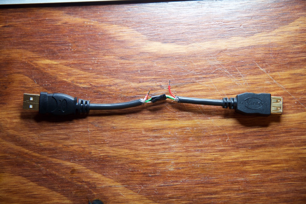
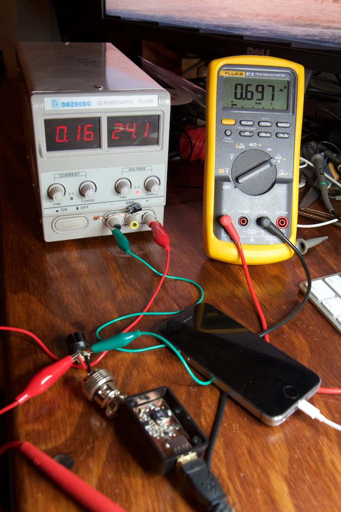
In order to test how well everything was working, I took apart a USB extension cable and modified it so that I could take series current measurements:
For a baseline comparison, I took a quick current measurement of my phone getting charged by my Anker battery. Note that the phone has to be below about 70% charge for this to work. If it’s above 70%, it will enter constant voltage mode where the current draw will start dropping on its way to full-charge:
As expected, the phone charges with almost exactly 5W of power.
Plugging into my circuit produced this:
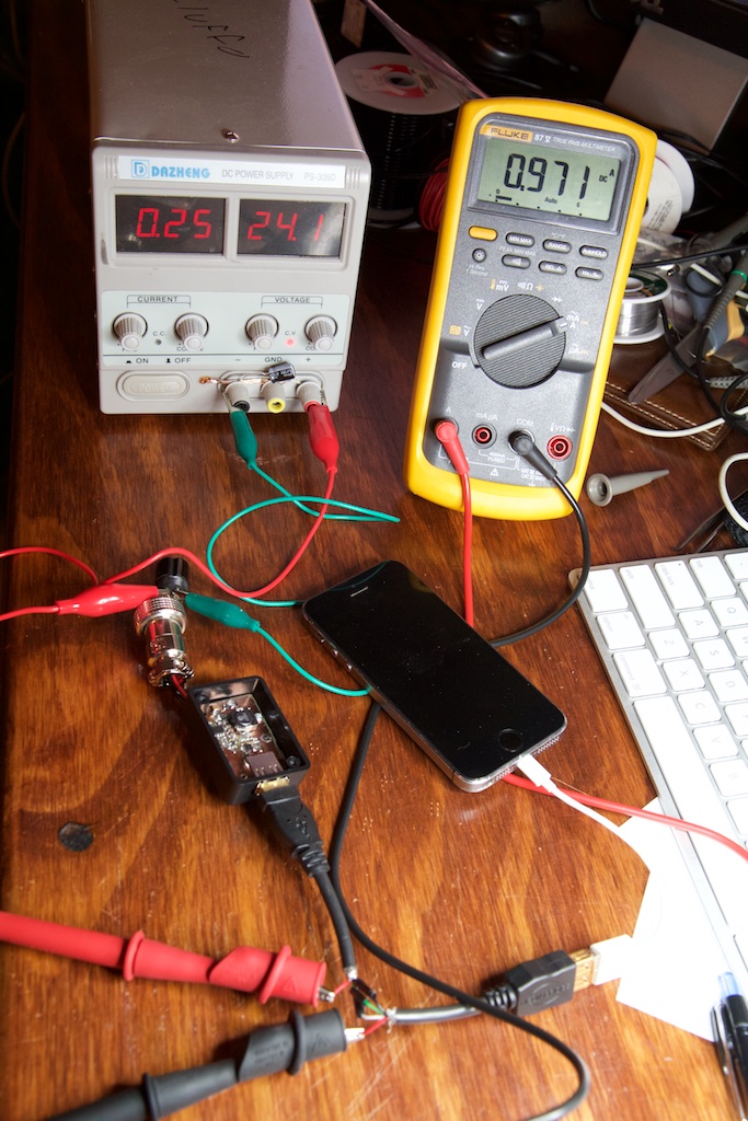 Hey, not bad! Except wait… unplugging the phone and plugging it back in gave me this:
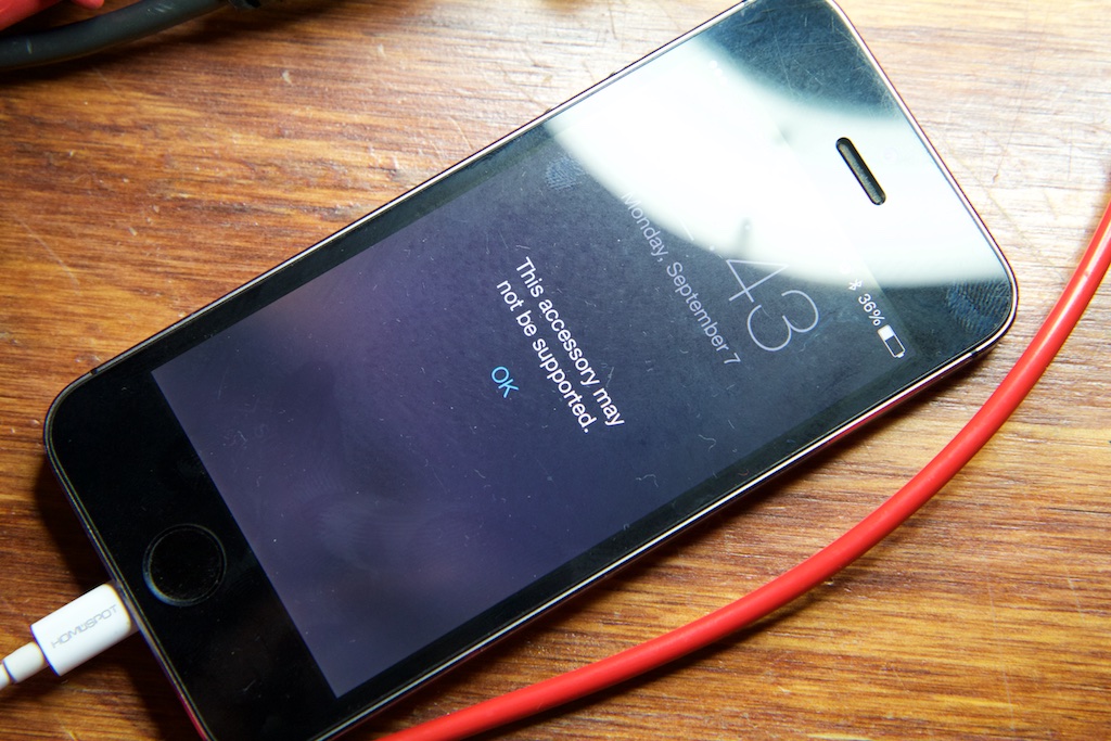
700mA charging. In fact, it seemed like it would only charge at the full rate about 10% of the time. Sometimes it dropped to 200mA and displayed one of these:
So for some reason, the phone wasn’t consistently able to negotiate the proper charging speed and would either drop to a lower speed or drop all the way to the minimum speed and indicate that something was wrong with the charger.
Fragile circuits
Before continuing, I’d like to point out that a lot of the problems and frustrations I encountered during this investigation were largely due to my fairly haphazard way of dealing with circuits. A lot of times, you might see me just poke around a circuit board to get measurements, but that doesn’t really fly with power electronics dealing with multiple amps and 24 volts.
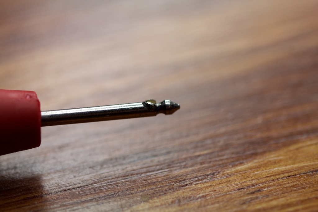
In a typical low power circuit, a gentle accidental prod with a multimeter probe might cause a circuit to warm up a little, but nothing bad usually comes of it. This time, even a tiny graze with a short is enough to cause permanent, immediate, and sometimes spectacular damage.
For example, the output of the battery doesn’t appear to have any kind of over-current protection. Either that or the normal operating mode of the battery involves driving an insane amount of current (more likely). See exhibits A and B:
If the output of the buck is under load and you aren’t careful when connecting the 26V input power, bouncing of contacts can cause inductive ringing on the input which can exceed the chip’s 28V input limit and blow it up. Literally:
But perhaps the worst thing to happen was this:
At some point during testing, I must have shorted something which broke the charging circuit on my iPad 2. I’m not sure what’s going to happen when the final 30% drains from its batteries, but it’s likely that it won’t be of any use after that. I looked into fixing it, but there’s no separate battery charging PCB, and the main logic board replacements aren’t very cheap.
Let’s just say that it’s awful good timing that they announced new ones last week…
As a result of this iPad trauma, towards the end of this investigation, I started being more careful and performing tests with purpose-soldered setups. You’ll probably see a combination of haphazard and careful in the images throughout this post.
TPS2511
Given that the phone was having trouble negotiating a charging current, my first target was the TPS2511. I suspected that perhaps something was wrong with how I had it configured or that perhaps it didn’t support the iPhone’s charging scheme.
There are a few options when wiring up the TPS2511 that allow you to select 5W or 10W charging mode.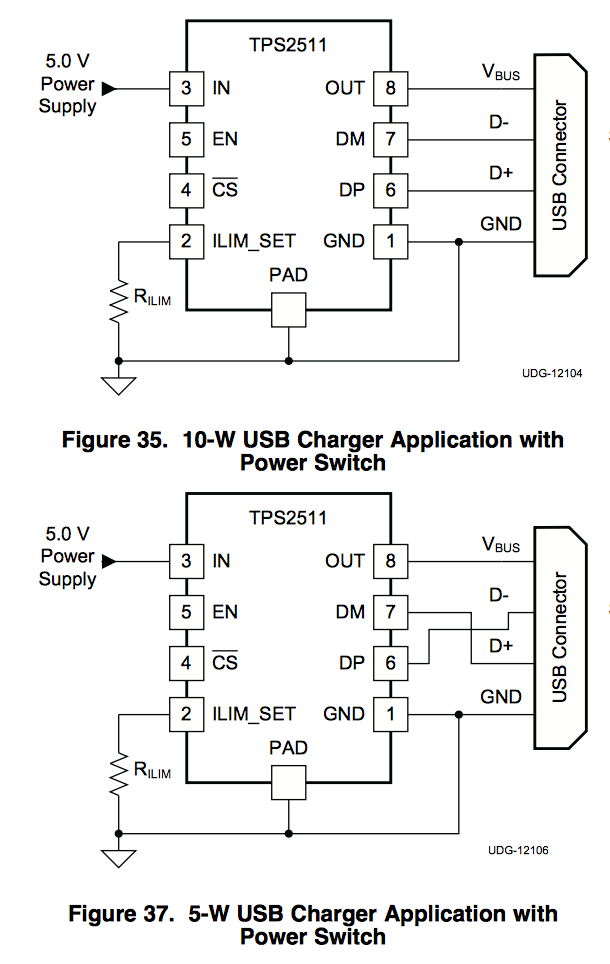
But that would wouldn’t explain why my iPhone wasn’t charging considering it only needed 5W. Furthermore, I think the “failure mode” for configuring this wrong would be the iPad (which normally needs 10W) charging at a slower 5W pace.
For a while, I also had a suspicion that my layout allowed one of the data lines to touch the housing of the USB port, but the problem still persisted after fixing that.
Buck
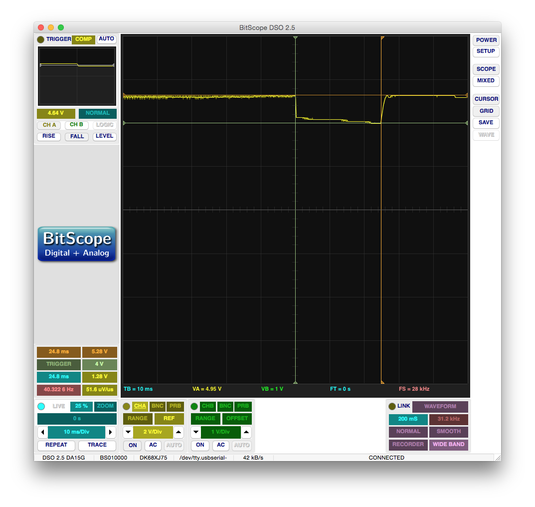
After poking around for much longer than I should have, I decided to crack out the oscilloscope to see what was actually going on. The 5V rail coming out of the SC4525C looked like this:
Okay, now we’re getting somewhere. It’s reasonable to expect a small dip or some minor instability when connecting a large load to a power supply, but a dip of over a volt on a 5V rail is bad.
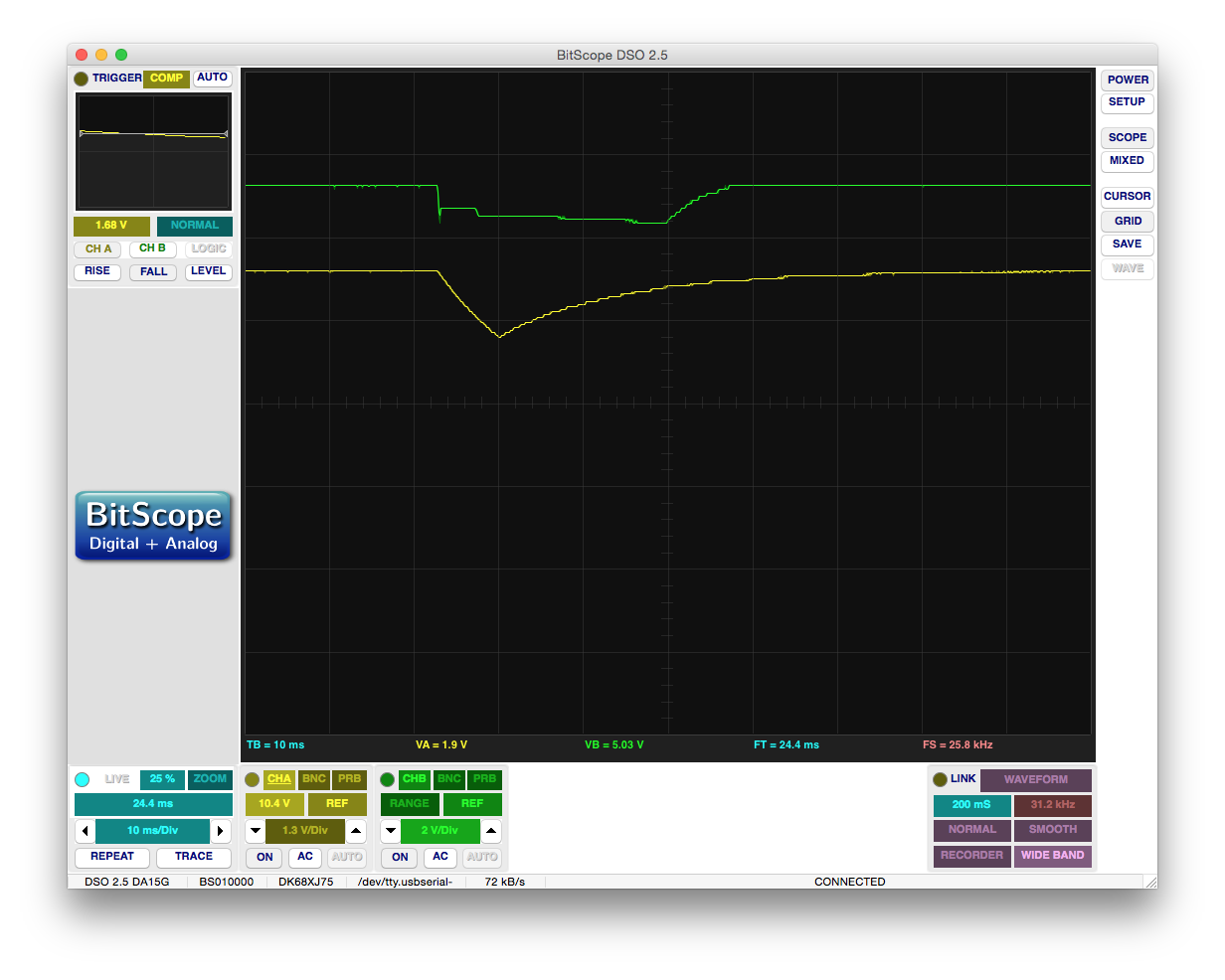
I tried fixing it with a 100uF electrolytic cap across the output, and while this did help a little:
It didn’t feel like a good solution, so I removed it.
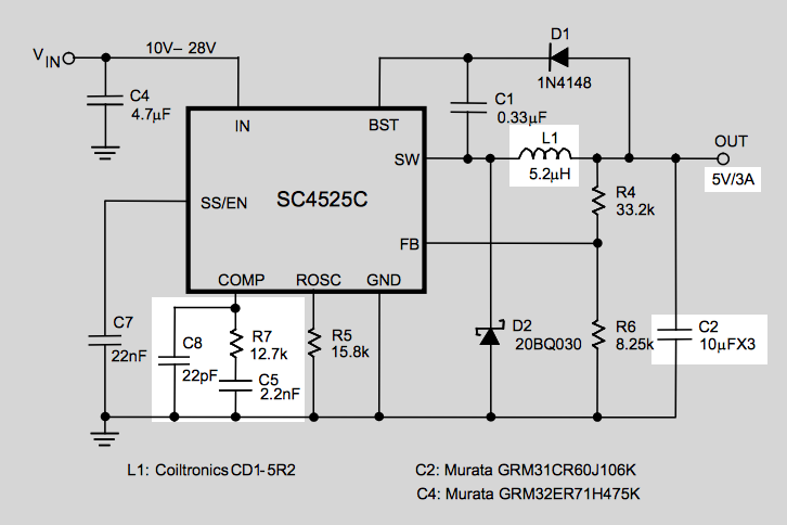
I started to wonder if stepping 26V down to 5V with a 1-2A output was unreasonable, but that was literally the example application shown on the first page of the data sheet:
Looking into the rest of the data sheet, I found something interesting and decided to take a look at the Soft-Start pin:
The SC4525C’s Soft-Start pin is intended to be connected through a capacitor to ground. Under normal operation, the part will charge that cap to a certain voltage. During times where the buck converter’s maximum output current is exceeded, it will suck charge out of the cap at a certain rate. By monitoring the voltage drop on the cap, it can determine when it has been operating in an over-current state for an extended period of time and decide to shut down safely.
Looking at this trace, it seems that as soon as I connect my phone, the chip freaks out and almost immediately shuts down. Because 1A was well below the maximum current draw of the part, I suspected that there had to be some kind of instability causing the problem.
Compensation
Now when I say “electrical hell,” this is most of what I’m talking about.
The SC4525C contains most of the bits necessary to create a buck converter, but there are some aspects of buck design that can’t be accounted for up front. A small network of resistors and capacitors connected to the compensation pin of the chip allow a designer to program the chip’s feedback system to function well with his or her chosen buck converter components.
Almost immediately, I noticed that the example circuit shown on the first page of the schematic:
does not appear to use the values listed in its own table of suggested parts:
In fact, if you run the numbers on the formulae found elsewhere in the data sheet, you still won’t quite get the values in the table, though you’ll definitely be closer than the example schematic.
Since I had used the values provided in the example, I was convinced that I had found the smoking gun. After swapping them out for the right values though, the circuit’s performance was the same.
Because the provided formulae require you to know the ESR of the output cap of your buck converter, I was concerned that maybe the table assumed the wrong value. This lead me to dig in hard to see if I could understand exactly what this compensation network was trying to do and how an incorrect ESR value might explain the behavior I was seeing.
When I set out to write this project up, I was planning on doing an entire section on compensation networks and how they function. This turned into a larger endeavor than I was anticipating as understanding their purpose involves an intimate knowledge of feedback control and system analysis. These have never been my strengths:
Ultimately, the compensation network was not responsible for the problem I was encountering, but since I had already scratched the surface, I wanted to take a deep dive. This set off two weeks of furious head scratching that served as a bit of a reminder that it might be time to review some of the stuff I tried to learn in undergrad now that it’s turning out to actually be useful… Who’d have thought!
I would like to eventually do a write up of compensation networks if only for my own edification, but I’d also really really really like to get this thing off my desk. Some other time.
Current Loop
I recently decided to get my ham radio technician license (if you ever hear from KG7VYH, say hi), and one of the questions they pull from the pool for the exam is:
As I found out during this project, A is definitely not the answer.
At around 2AM one night, I started to notice a small amount of noise appearing on the feedback pin of the SC4525C that was not present on the output of the buck converter. This meant that somehow the feedback pin itself was producing noise which could very much explain the odd behavior I had been seeing.
Right around this time, I slipped up and produced the spectacularly exploded chip seen earlier in this post. I decided to call it quits for the night and go to bed. Five minutes of half-assed eye-closing later, and I was back on my phone reading over the data sheet again. Somehow, this was the first time I noticed this note on page 16:
I’m no stranger to minimizing loop inductance. I’ve run into it before on a yet-to-be written-up project. If you follow me on Twitter, you may have seen this:
Because schematics do not “accurately represent the lengths of wires,” it’s often easy to forget how critical short current paths can be for the performance of high-power, high-frequency circuits. This is especially easy to mess up when it comes to connections which are maintained by large copper pours such as ground planes.
In the above example, the current trying to get from A to B has to travel half of its journey on a roundabout trek around the top layer ground plane before dropping to the bottom layer to complete it. I made a point of peppering vias between these two planes throughout the PCB, but I didn’t pay any special attention to the critical current paths that would be using those vias.
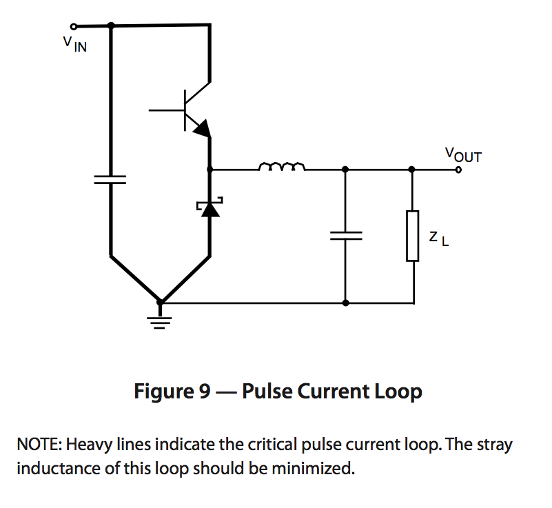
That circuit was also a buck converter, and on the schematic, the current loop looked like this:
It’s a little weird to think of current traveling through capacitors, but remember that this is AC current. When the controller pushes current into the inductor, some will flow out the other side, through the capacitors, and back to the source (more specifically through the source’s bypass capacitors. Not pictured here).
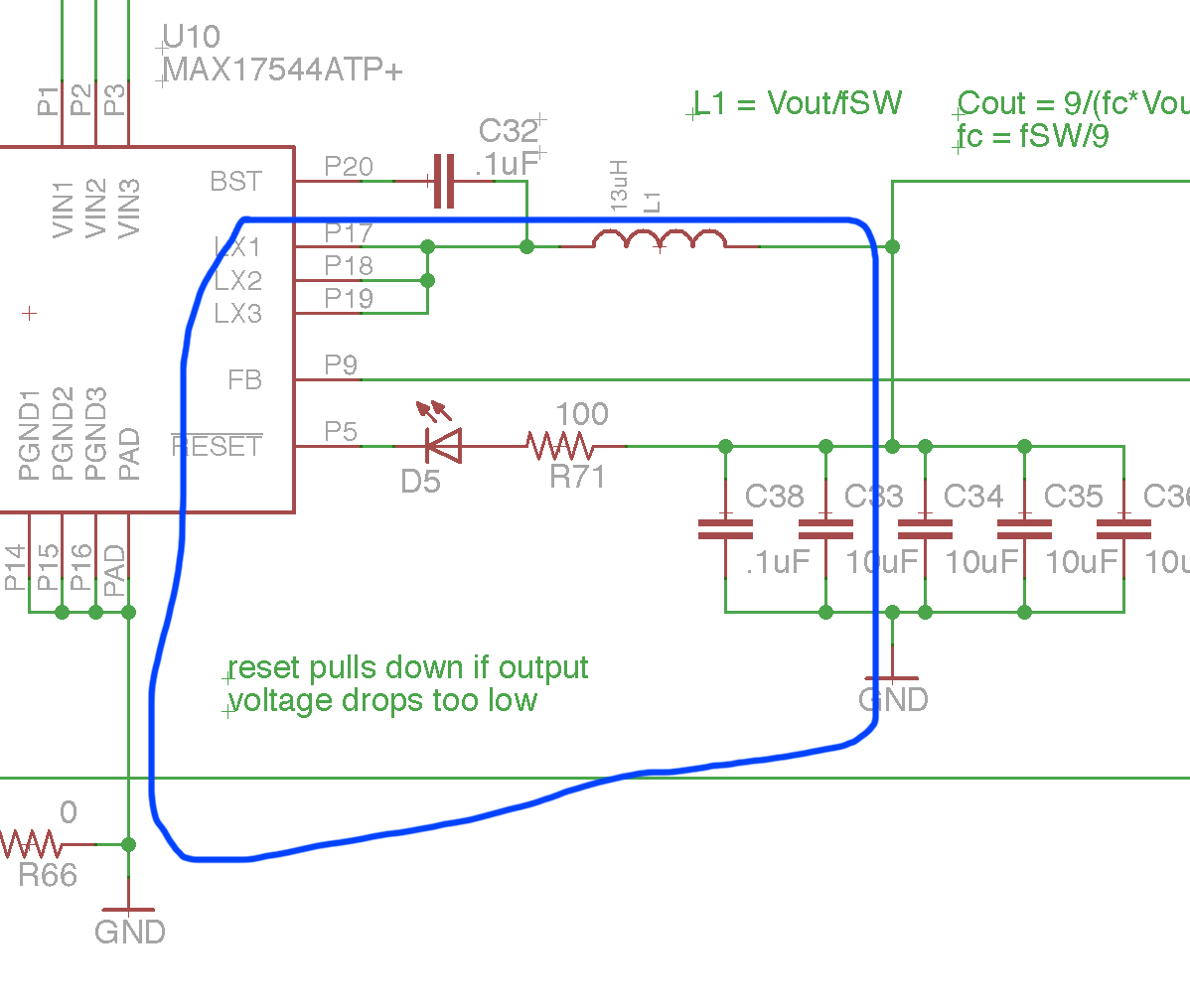
This is why this time around, I decided to optimize this current path in my design:
What I failed to realize was that I was optimizing the wrong loop!
While it’s a good idea to keep all loops as short as possible, the output loop will be generally tolerant of parasitic inductances. Heck, a large portion of the loop actually is an inductor.
I should have been optimizing the input loop.
The current in the output loop (“ripple current”) will rise and fall every cycle, but the gigantic inductor in the loop will slow this current ramp. The is fundamental to how a buck converter works.
In the input loop however, certain elements can go from zero current to several hundred milliamps of current in an instant. This is especially obvious in the SC4525C which is not a push-pull driver and depends instead on an external freewheeling diode to maintain inductor current.
For the first part of every cycle, current will travel from the voltage source/input cap, through the chip, and out to the inductor.
For the second half, the output of the controller shuts off, and current instead comes from the freewheeling diode, D1:
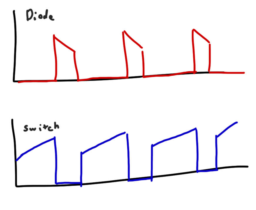
If you were to plot the current in the diode and chip, it might look something like this:
You can see that the peak of the currents follow the gradual rise and fall of the inductor current, but ramping up to those peaks is much, much faster, and that current needs to be available immediately.
Inductors fight rapidly changing currents, so if there isn’t a very good source nearby (like the input cap), the inductance created by the longer path will act to slow down these current spikes and round off the edges in the plot above. As the data sheet points out, it’s critical to keep that path short.
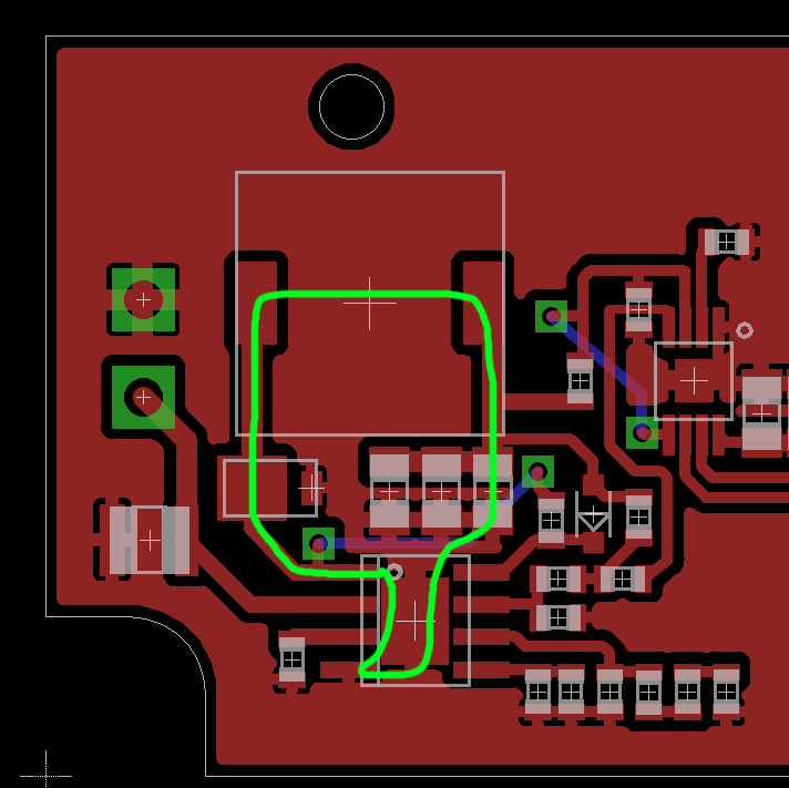
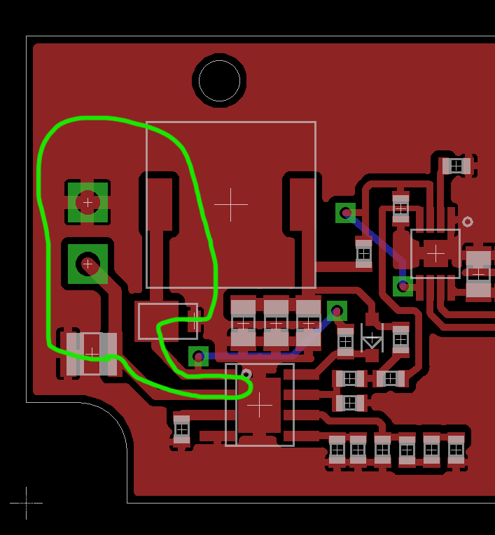
Let’s look at my path:
You know, it doesn’t look absolutely terrible, which is probably why I didn’t think much of it during design. Regardless, even that small, maybe 1″ current loop was enough to disrupt operation. Rearranging the cap like this immediately solved the problem:
1A, 2A, no problem. No matter what I threw at it, this thing was suddenly performing like a champ. Also, I hope you appreciate my tower of output caps that I had added when looking at the compensation network.
This solution could also explain the noise I was seeing on the feedback line. With no capacitor nearby, the high current spikes could have sucked charge out of the controller’s power rail causing its voltage to dip dramatically and upsetting its internal analog components.
With that problem FINALLY squared away, it was time to re-design the PCB and get testing!
Performance
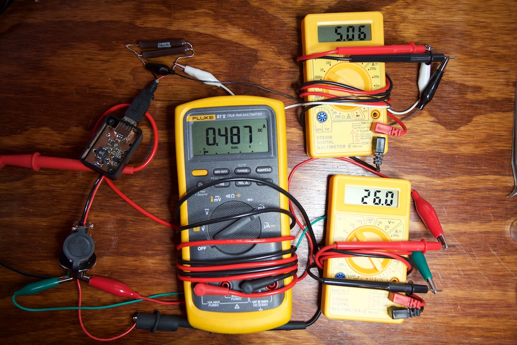
This is when it’s nice to have a handful of multimeters.
With a 26V, 487mA input, the buck converter provided 5.06V to a 2.5
![]()
load. That works out to:
![]()
![]()
![]()
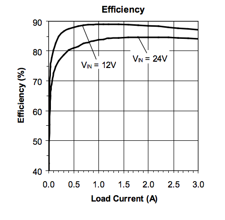
Hrm…80% doesn’t look too good. The data sheet estimates around 85% efficiency for a 2A load and 24V input:
Remember what I said about how the TPS2511 can boost up the output voltage when the current draw is high? This is exactly why. If you measure the voltages inside the box, it paints a different picture:
The voltage drop across the beefy GX-20 connector is negligible, but it looks like we lose quite a bit across the TPS2511 and USB connector. Using these new values:
![]()
![]()
![]()
![]()
Perfect!
Getting hot
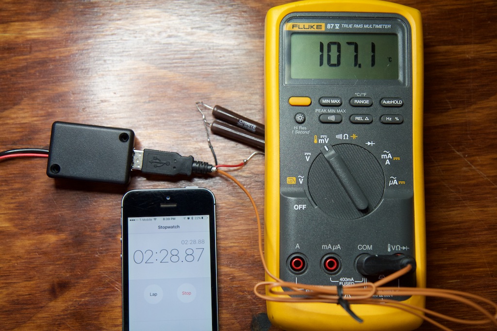
Even with 86% efficiency, 1.77 Watts of power is being turned directly into heat. The box gets hot. The recommended ambient operating conditions for the SC4525C as specified by the data sheet go as high as 105C, but I had a feeling I was getting hotter than that given how uncomfortable it was to hold the box and how its output went to zero after a few minutes due to thermal shutdown.
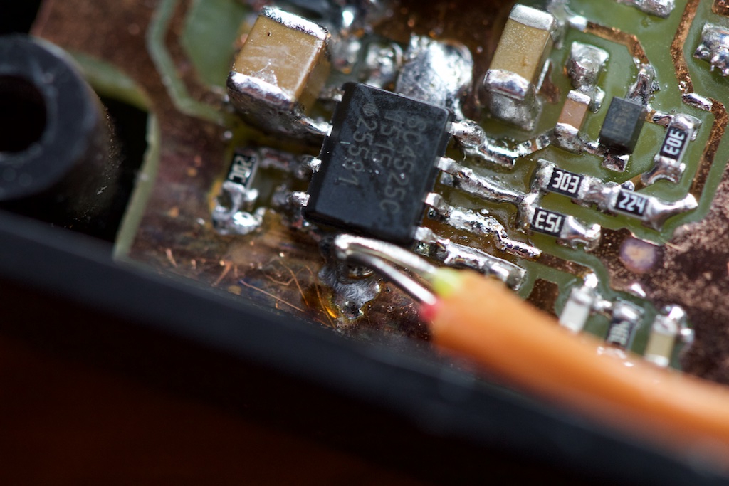
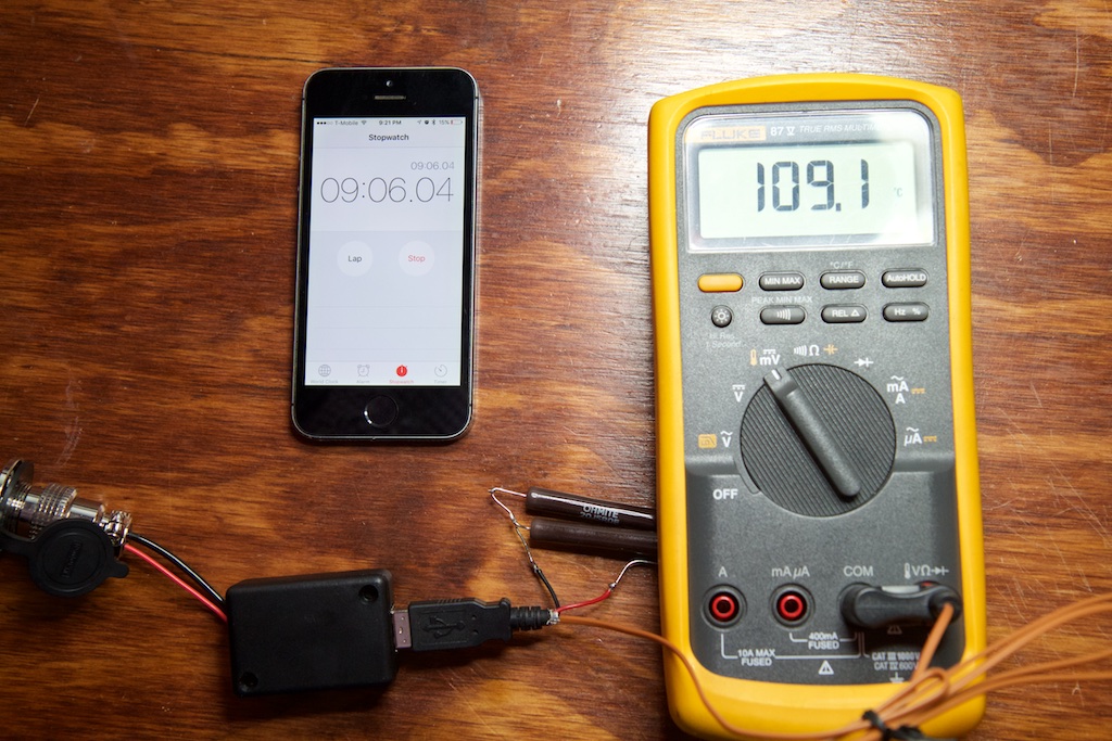
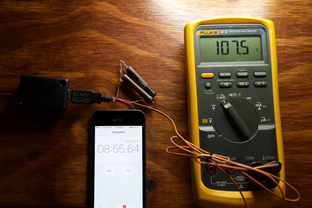
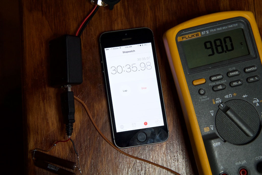
To get an idea, I tucked a thermal probe right next to the chip, plugged in a load, and started a timer:
Granted, I hadn’t let the box cool all the way to ambient temperature before running this test, but even starting from 30-40C, that got really hot really fast.
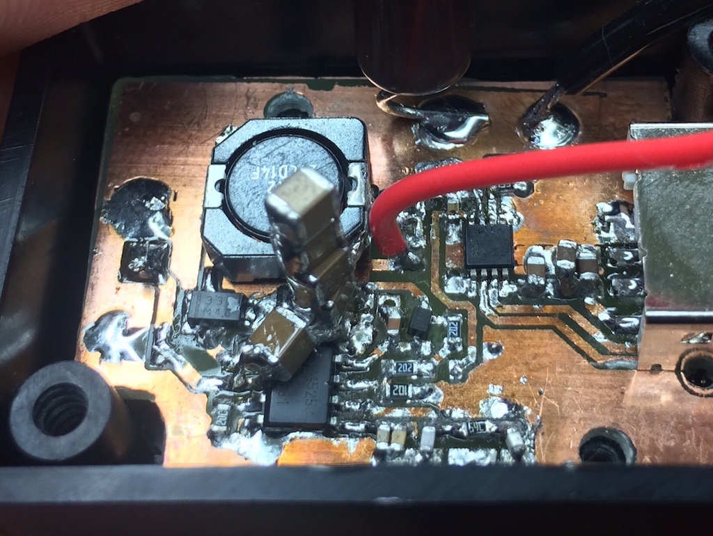
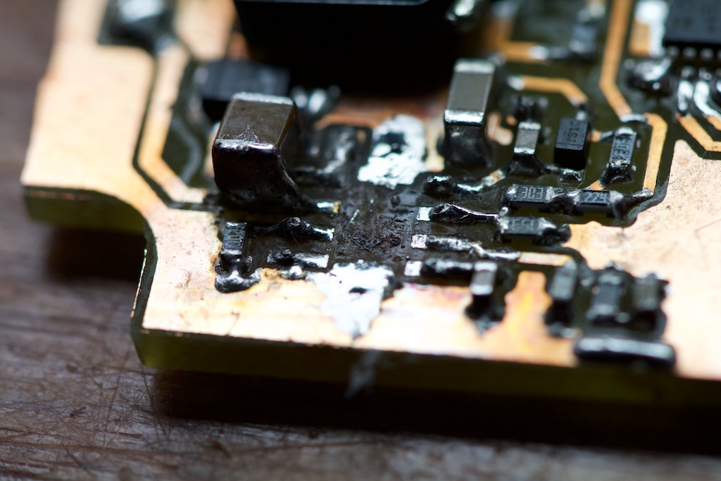
So it seems that a lot of heat was pooling up inside the chip. One possible explanation could be a bit of damage I caused during a rework:
For some reason, one of the chips I blew up along the way got really attached to the ground pad and decided to take it with. Even if I hadn’t ripped it off, that pad wasn’t going to help too much with heat anyway due to how I designed it.
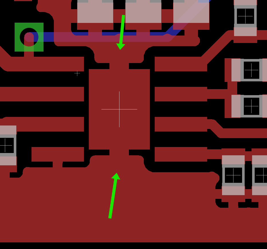
When you create PCB footprints, you have the option to make “thermals” which maintain electrical connection, but increase the thermal resistance by removing some of the copper around the pad. The intended purpose is to aid in soldering as it can be difficult to get solder to stick to a surface where any applied heat gets quickly sucked away.
In this case though, I actually want heat to get sucked away. Next time, I won’t use thermals. In the meantime, I attempted to repair the broken pad with a bit of solder wick soaked in solder and placed under the part:
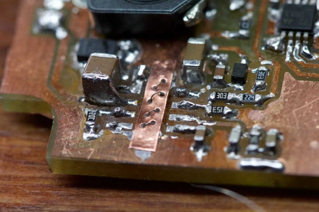
Though this worked to some degree, I thought it could use some improvement. For starters, the wick wasn’t very flat, so only a portion of the ground pad on the part was making good contact. Furthermore, even if the board hadn’t been damaged, there just isn’t much of a thermal path in the ground plane.
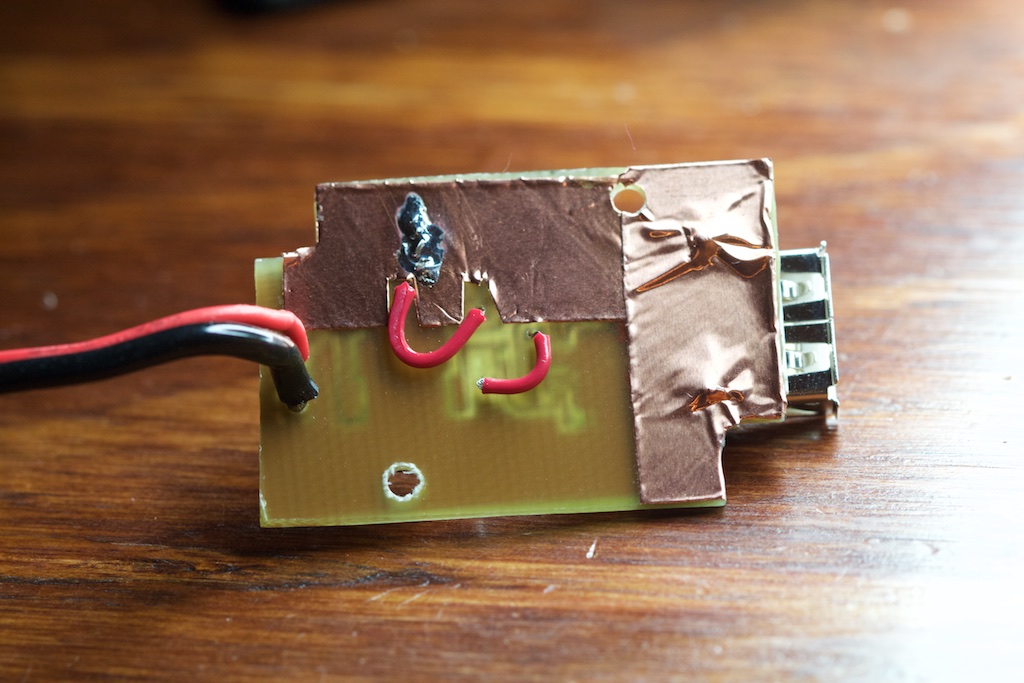
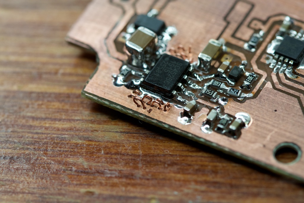
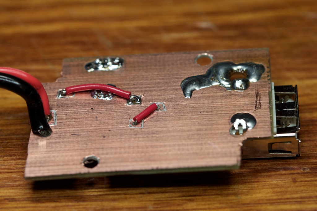
In a multi-layer design, something like this might be remedied by running a bunch of vias to other planes in the board to improve the overall surface area of the copper. Since this was a one-layer board, I had to improvise with some copper tape and wire:
How’s that for ground plane stitching! HAHAHAHAHAHAH!
Though I only after I did this did I read another line on the magical page 16 of the data sheet:
Oh well. let’s just see how well it does:
It didn’t prevent it from overheating, but it definitely slowed it down considerably.
Not ready to give up quite yet, I made one more version of the board. This one had a flat ground pad under the part with no thermals and then a huge number of vias peppered around the outside.
I used two-sided PCB this time. I planned to actually route the two traces on the back of the board, but I messed up a bit during the developer step, so I just isolated the relevant vias with a razor blade and ran the traces using wire again.
After dousing my ground plane stitching with solder, it was time to run the thermal test again!
Hrm…not much better.
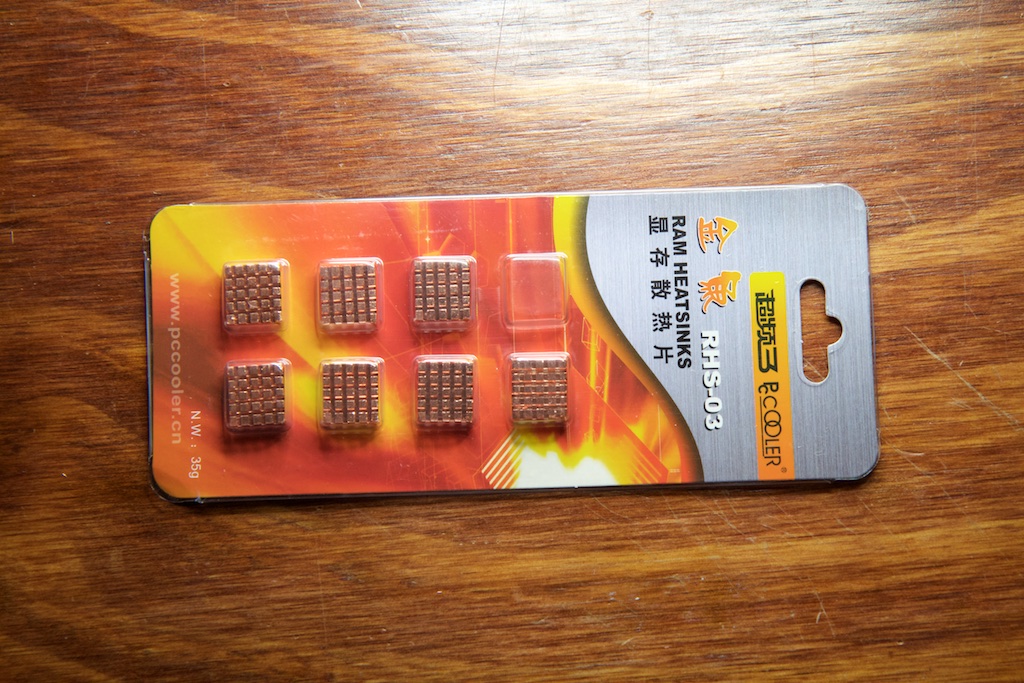
Alright, trying to dissipate heat inside a black plastic box with zero ventilation might just be asking too much. Time to break out the big guns:
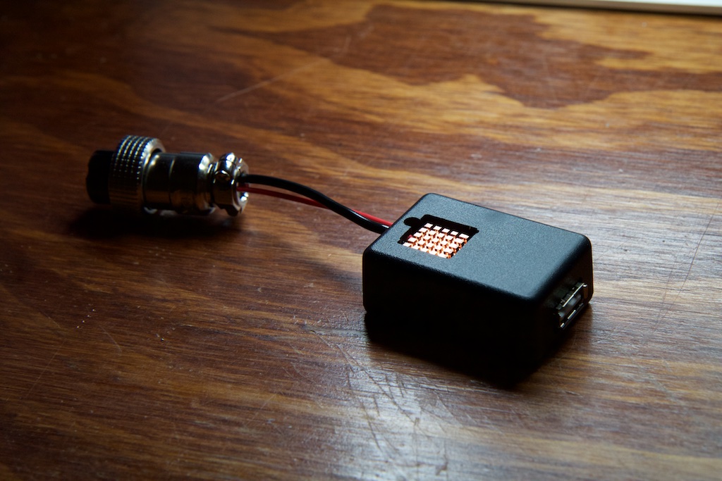
These little heatsinks have adhesive backs, so I stuck one on the ground plane on the bottom side of the PCB and cut a small ventilation hole. I also moved the cable hole from the bottom to the back. I tried to get the heatsink as close to the part as possible, but space was tight. It ended up right underneath the inductor.
With the heatsink installed…
Sweet!
The circuit reached steady-state at 98C, so after half an hour I decided to abort the test.
Though it’s towing the line of what’s electrically acceptable, it’s still technically under spec. And I should point out that this is in my apartment where the ambient temperature is already 22.9C (73F). I’d expect it to perform even better in colder environments.
Holding something that’s 98C is another story. The box is hot, and touching the heatsink with your finger almost immediately crosses the pain threshold. Still though, when the zombie apocalypse strikes, it’s better than nothing.
Conclusion
So there you have it, I managed to purchase two ICs and use them exactly as specified by their manufactures. Yay!
Really though, a lot of the struggle in this project happened off-stage. I already do a lot of rote engineering at work, so for my personal projects, I always hope to do something that is new to me and gives me an opportunity to learn. I was worried starting out that this project would be so simple that it wouldn’t even warrant a blog post. Every post needs some kind of challenge or problem to be interesting. Once I came across the compensation network thing, I was excited that I finally had something worth writing up, but it turned out to be far too complicated to dig into with all of the other stuff I have going on right now.
I will be writing that up at some point in the future, but for the time being, I still managed to learn some things even in this very simple project.
- Optimizing input current loops in switch-mode converters is critical. I’m using the SC4525C in a much more complicated project at the moment and have had some output stability problems there. I think the input current loop could be the root cause of my problems with my other circuit, and I never would have found it without a chance to isolate it in this design.
- Inefficient things get hot. I’ve never had a circuit before that got so hot by design. Efficiency has always been nice from a battery life standpoint, but this is the first time it’s been so critical to basic functionality. If I were to design this circuit again, I’d pay much more attention to heat dissipation by moving to a metal enclosure or including ventilation and a small fan.
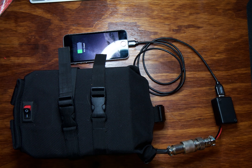
I’m not sure if I’m ever going to use this thing now that it’s done. My Anker battery can charge my phone around 7-8 times on a single charge which is pretty practical for most non-apocalypse scenarios.
I estimate that my bike battery can charge my phone about 25-30 times.

















Techspray ProWick #6 copper desoldering braid (4.9mm wide!) works well for me, when I want low-inductance, low-resistance, high current pathways. You can either lay it atop PCB copper and solder along the entire length and width, or treat it as an “air wire” that jumpers over traces and components. Don’t forget to insulate it if you do.
Linear Tech datasheets are great for layout tips for DC/DCs — Semtech parts are inexpensive but their design support leaves a lot to be desired (if you’re low volume).
The tips generally apply across converters as long as the topologies / control schemes are similar (voltage-mode, current-mode, constant on-time, etc.). Sometimes trade-offs have to be made; i.e. minimizing the size of the SW node helps with EMI, but you increase resistance as a result.
I use LT and Semtech almost exclusively these days, with the latter being primarily for cost sensitive stuff.
Pingback: Electrolytic capacitors and preserving a family heirloom | ch00ftech Industries
Vout=2.98V+(30kΩ×(0.009mA+.066mA))
let me know how you calculate the 0.009ma
That was a well-written article. As an EE myself, it’s refreshing to see obstacles overcome. Keep tinkering!
vcrkgq
suqayw