The moment you’ve all been waiting for! My super awesome guide on how to make these
 Theory
If you’ve ever developed film then you’ve taken part in a process very similar to UV sensitive PCB etching. The basic concept is to use UV light to soften and remove a substrate and use the remaining substrate to protect copper from an acid bath.
Shopping
- Copper. To start, you’ll need to purchase some special copper clad that is coated with “positive UV resist” substrate. I experimented with a few brands, and found MG Chemicals to be the best. The boards are coated with a highly-visible layer of substrate and are well protected during shipping.
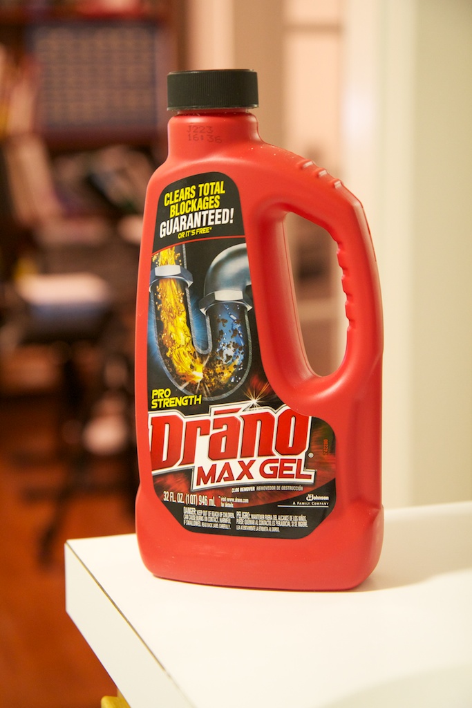
- Sodium Hydroxide (NaOH). NaOH will dissolve the substrate coating after it is exposed to UV light. This is actually pretty difficult to come by in a pure form. Apparently NaOH is used for making meth, so you can’t find it pure. It is one of the key ingredients in Drano though:
- UV Lamp. I bought a special UV lamp used for making PCBs, though I’ve heard you can just take the UV filter glass off of a halogen work lamp. The only issue with that solution is that it will get rather hot.
- Weight. You will need a UV-translucent plastic or glass weight to hold your artwork flat during exposure. Do NOT use the glass from the front of your work lamp if you go with that method. That glass will not pass UV light. That’s sort of the point…
- Transparency sheets. You can print on either laser jet or inkjet. Just make sure you buy the appropriate transparency sheets.
- Really small drill bit. I used .031″ These work best in high-speed drills like a Dremel. For best results, use a drill press.
Preparing/Printing the Artwork
I love that they always call it “Artwork”. Anywho, when designing your artwork, it’s important to remember that vias are sort of a pain in the ass to deal with, so try to minimize those in your design. Especially avoid placing vias under surface mount chips because it’s very difficult to make a hand-made via totally flush to the PCB, and you might not be able to solder down a surface mount part if it has a via under it.
When you’re done with your layout, you will need to set up your PCB layout software so that it only prints the things you want to end up in copper (i.e. not the silkscreen text, etc.). I use Eagle for my layout, and turned off every layer but Vias, Pads, Top/Bottom), and Dimension. The latter obviously doesn’t need to end up in copper, but it’s nice to have some point of reference for where your board is supposed to end. You can see my settings for the top layer here:
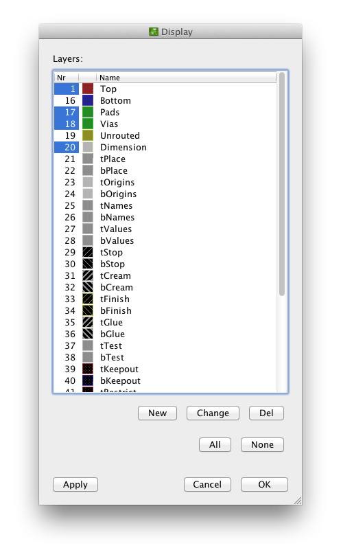 When you print the top layer, make sure you select “Black” and “Mirror”:
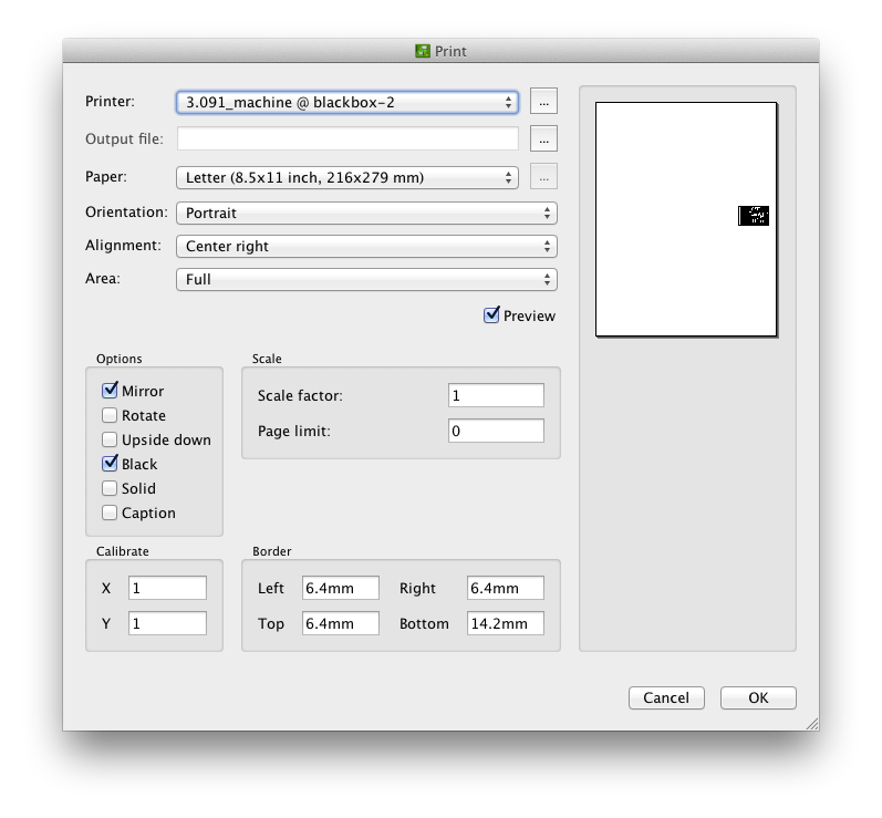 You might be wondering why “Mirror” is so important if you’re going to be printing on a transparent sheet of material, but I’ll explain that later. When you print the bottom layer, you will want to deselect “Mirror”.
You should now have two layers of artwork printed on two sheets of transparency.
Preparing the Board
Like I said, the MG chemical boards come in some pretty nice packaging. Each side is coated with a semi-adhesive protective layer and the whole thing comes in a opaque black bag (to prevent exposure during storage).
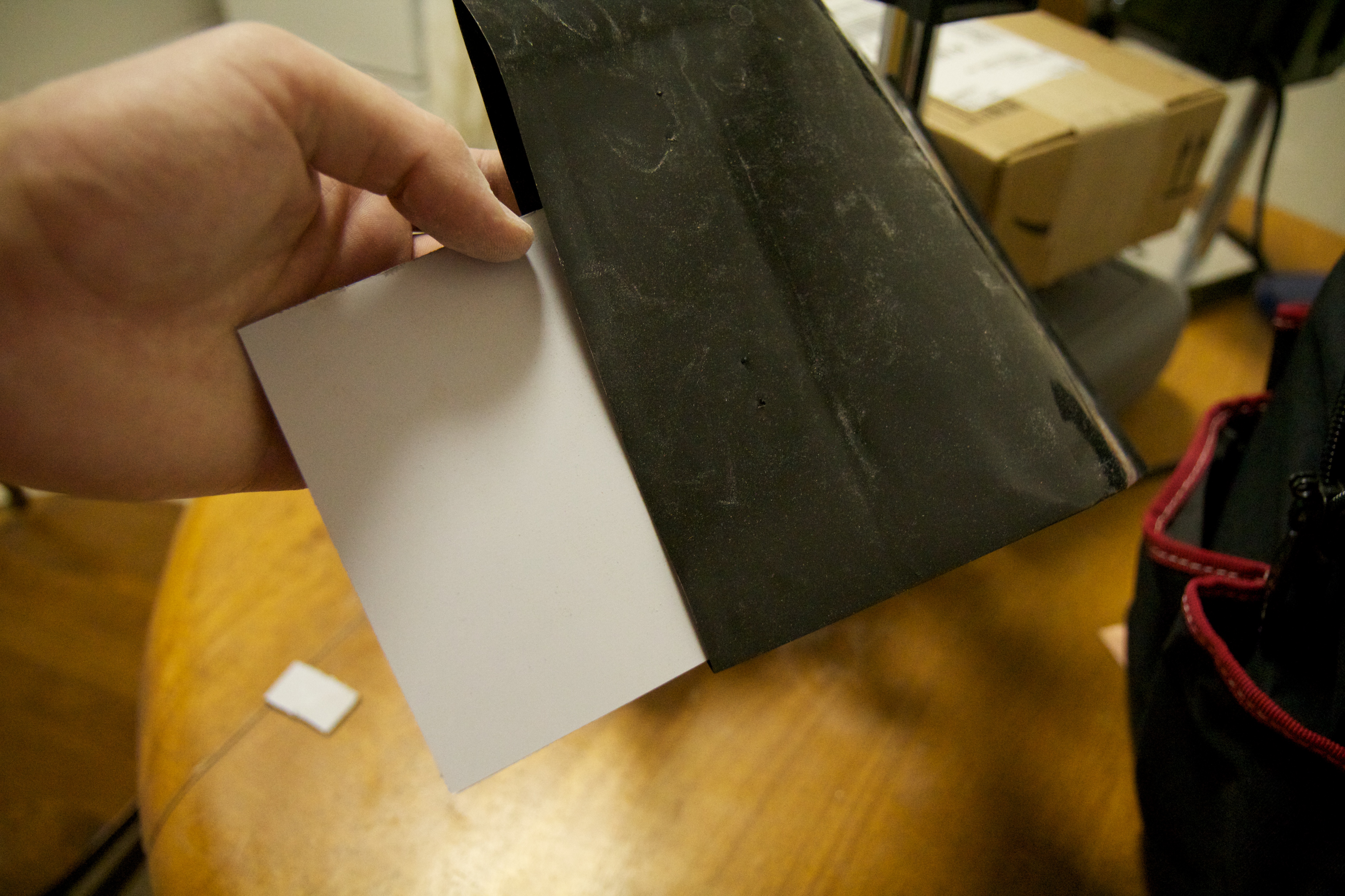 Mark your board where you will be cutting it. I used a pair of calipers which are handy for scratching precision marks in the protective coating.
 You then will need to cut your PCB down to size. Some people use tinsnips for this, but I opt for a Dremel tool.
 Be careful that you don’t let the shank of the dremel scratch your PCB. You can see that this happened in the upper right corner of the board. Luckily, this wasn’t in a particularly important location as far as my layout went. Also be warned that this method will produce tons of fiberglass powder. Breathing this stuff in isn’t a good idea, so work in an appropriate environment and wear a mask if you have one.
The end result:
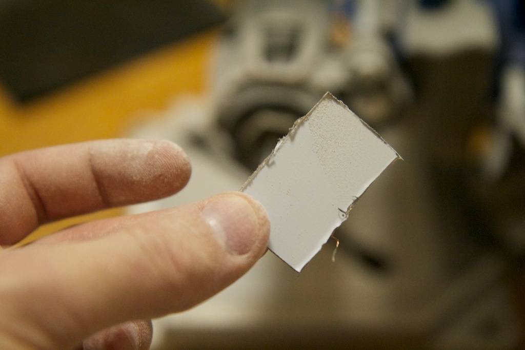 The edges are a little hairy, so maybe next time I’ll give myself more leeway.
Aligning the Artwork
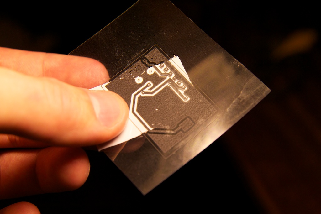
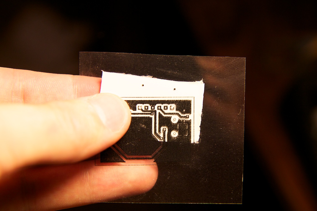
Remember what I said before about mirroring the top layer? The reason that is important is because you want the actual artwork to be as close to the PCB as possible. If you have the artwork on the side of the transparency sheet opposite the PCB, there is a possibility of light leaking in sideways and causing the edges of your copper to be “fuzzy” which can result in poor etching. It should be pretty clear which side goes towards the PCB because it will have a matte finish as seen here.
And when aligned properly:
Now, part of what scares everyone about making two-layer PCBs is lining up the two layers. I’m here to tell you that this actually isn’t that difficult especially when the board is small. All I had to do was use my drill press to drill two reference holes through the artwork and board. These holes can then be used to align the other layer. The farther apart they are, the easier it is to prevent rotational misalignments.
 Exposure
This next step is probably the most time consuming part of the whole process. You’ll need to start by carefully removing the protective layer of one side of your PCB. It’s best to do this at night or at least in the shade, because the Sun can be a pretty awesome source of UV light, and it can give you some undesired effects.
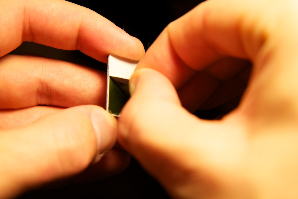 Then, align the artwork sheet with the PCB and secured it with some Scotch tape.
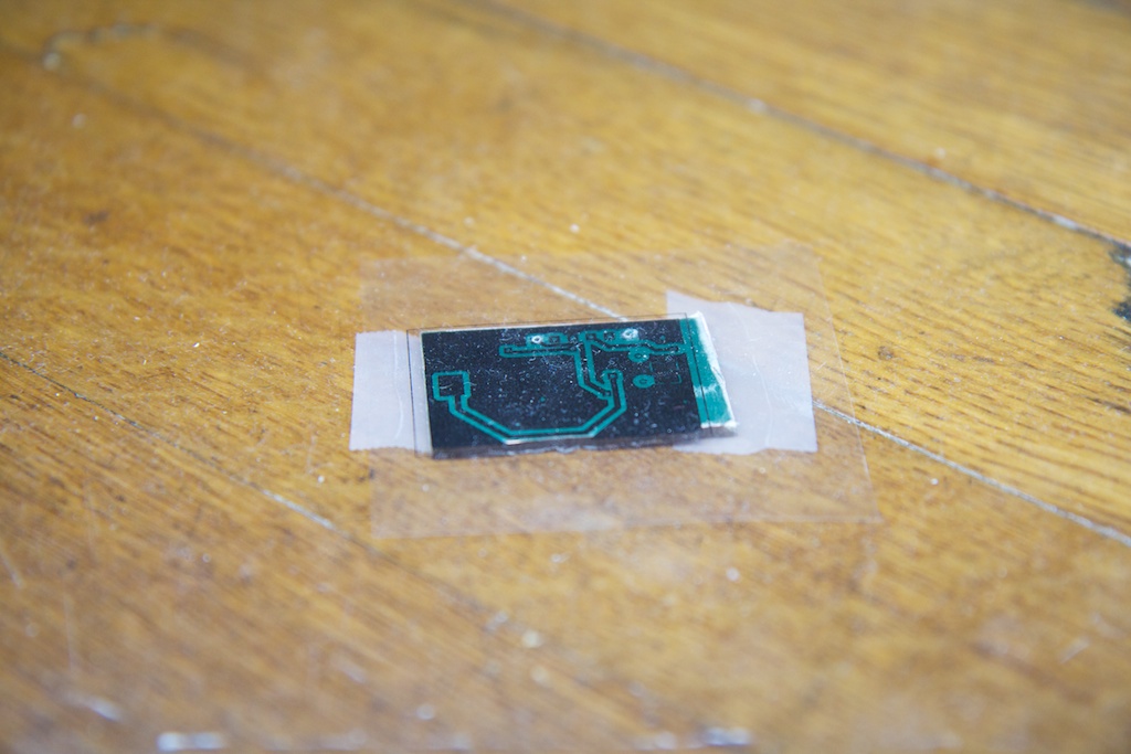 And placed it under a weight under UV lamp:
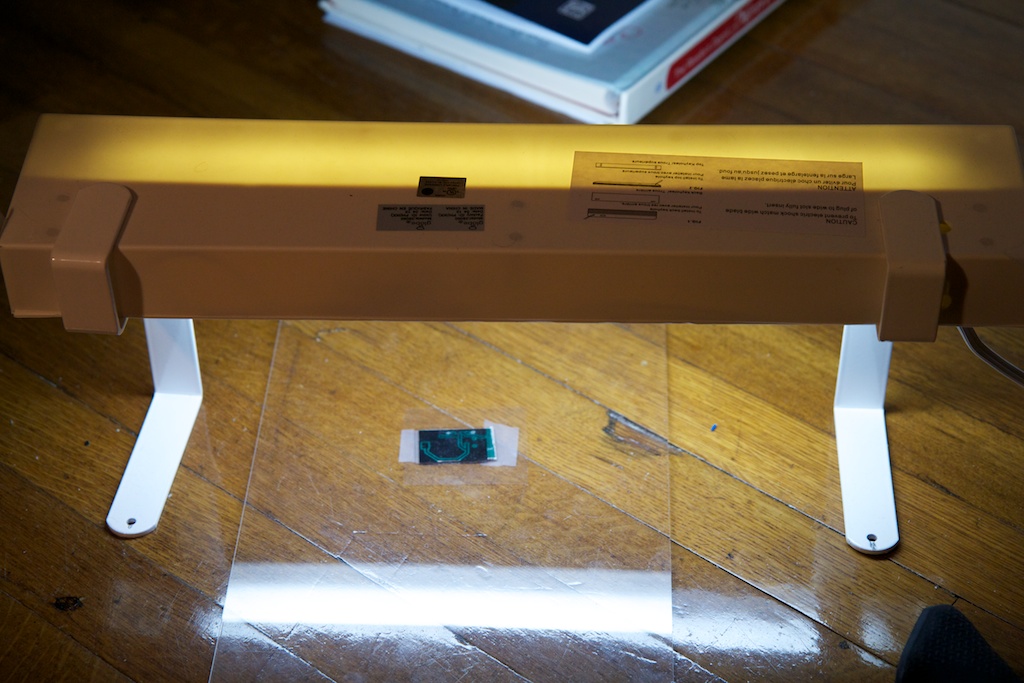 Now you wait. How long? That’s a good question. I found best results when waiting for around 15 minutes. If you don’t wait long enough, there will still be substrate on your board after developing. If you wait too long, you will end up washing all the substrate off during the development process. It’s pretty hard to wait too long though, because that would require enough light to seep through the black portions of your artwork to expose the substrate. If you’re low on toner, this can actually be an issue. Still, it’s best to err on the long-side.
If you really want to be scientific about it, print out some dummy PCB artwork and expose a test-PCB making sure to expose different parts of the board for different amounts of time. You can do this by covering most of the board with a piece of black paper and moving the paper back by a cm or so every two minutes. When you finally develop the PCB, you’ll notice some banding between areas with different exposure times (from two minutes to, say, twenty). The band that looks the best will correspond to the amount of exposure time that will produce the best results with your setup. Photographers use this “test strip” method in darkroom photography.
While waiting, I recommend making a bowl of mac and cheese, grabbing an blackberry IZZE, and checking out Star Trek: The Next Generation which is free for the watching if you have an Amazon Prime account.
 In this episode Troi falls for a handsome alien who steals her womb and Worf strikes a woman and scolds Alexander for eating cooked meat.
Once your 15-or-so minutes are up, do the same with the other side of the board being careful to align the artwork with the holes you drilled before.
 With both sides finished, it’s off to development.
Developing the PCB
This next step is probably the coolest one. You will need to prepare a solution of PCB developer. I found that one part Drano Max Gel and one part water worked pretty well. It is possible to over do it with developer concentration though. With some brands of PCB, I’ve had my developer wash all of the etch-resist clean off because it was too concentrated. Because of this, make sure to record what concentration you are using so you can make adjustments on your second trial.
Using a pair of rubber gloves, submerge your PCB in the developer and carefully rub it with a gloved finger or a foam sponge (be careful though, Drano can dissolve some types of foam) as seen in this video:
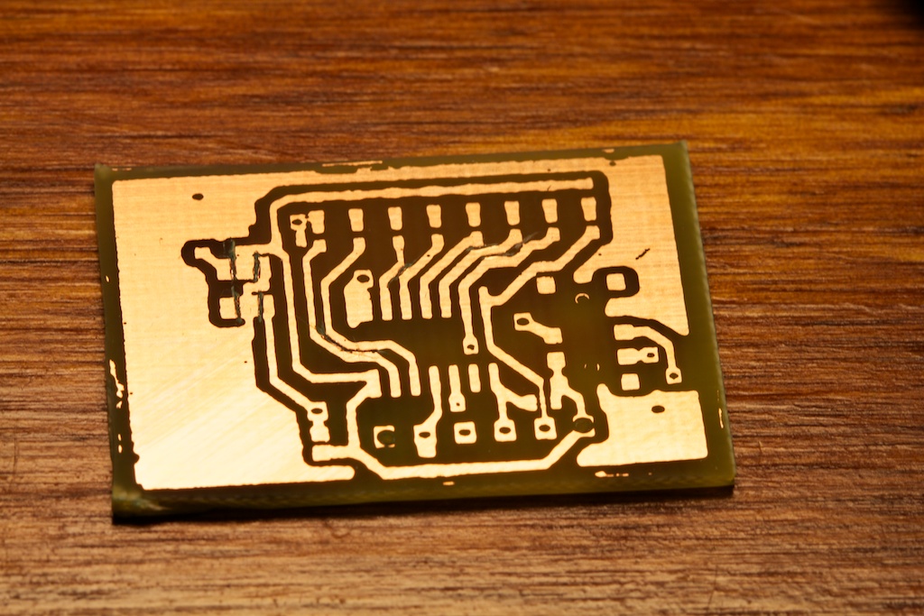
You should keep doing this until your board looks something like this:
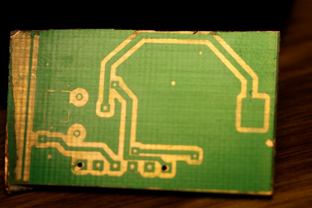 This is where having a nice dark colored substrate is handy; you will need to make sure that there isn’t any substrate left where you don’t want it. Bear in mind that even with the dark stuff, you can still have some semi-transparent layers. These thin layers will protect your copper and greatly increase your etch time which can lead to all kinds of problems.
If your developer still leaves some amount of substrate down where you don’t want it after a lot of soaking/scrubbing (more than 5 minutes), you probably didn’t expose the PCB long enough. You can try to re-apply the artwork, and expose for longer, but I haven’t tried this, so I can’t make any promises. It’s probably better that you just start over at this point.
Etching
The etching process is a pretty time consuming one. You can read tons of my other posts about PCB etching such as this one which should give you all the details. Despite what others on the internet say, my etching process still takes like three hours.
Finishing up
Unfortunately, I didn’t get any photos of the rest of the process, so I’ll have to describe it in text. Once your PCB is finished etching, you’ll want to wash off the remaining substrate using some acetone. You don’t need a lot, as it should come off fairly easily.
Then, you’ll need to drill all of your holes. I used a .031″ drill bit with a tabletop drill press. This is a pretty easy process, as the little copper vias should guide your drill bit into the holes it needs to drill. Keep in mind that you will probably miss a hole or two while drilling, so be very careful to double check that every hole is drilled before moving on. It might be a good idea to count the holes as you drill them and make sure that the count is the same on your artwork.
Finally, you’ll need to make vias where appropriate. I haven’t really ironed out this technique yet, but I had decent results with cutting small pieces of wire and soldering them into the holes making sure that they had a good joint on both sides of the board. You’ll have to be careful because heating up one side of such a short piece of wire is sure to melt the solder on the other side which will cause your wire to fall out. It’s a good idea to lay your board down on something flat and heat resistant while doing the second side.
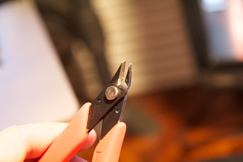
Making these completely flush is nearly impossible, but you can get pretty close using a good pair of angle cutters like these from Xuron:
 Conclusion
Well, there you have it. It’s certainly not the most cost-effective method for making PCBs, but I’ve found it to be one of the most reliable once you get the kinks worked out in your process. Expect to mess it up a few times, but once you get it right, it’ll be pretty easy to repeat your results and you’ll be whipping up board left and right in no time.

