So, after making the shutter shades that made a sensation all over the web, I had a lot of left over electroluminescent wire, and decided to do something with it:
Boom! 100% safer!
EL Wire
For those of you just joining us, EL wire is basically a simple coaxial wire with a special phosphorescent insulator between the conductors. When high-voltage, high-frequency AC current is passed down the wire, the insulator fluoresces and lights up. EL wire is fairly cheap, very flexible, and it comes in a variety of colors. I bought a pack of five 10-foot sections of colored wire with five power supplies off Amazon for less than $50.
Supplies
Like most things made in China, the power supplies that I got with my wire were incredibly cheap. One of them was dead on arrival due to a bad solder joint, and all of them were made out of that really crappy PCB material usually reserved for super cheap toys.
So it came as no surprise that they weren’t super reliable when I attached wire to my bike and started moving around. I found that every time I went over a bump, the supplies would shut off and refuse to turn back on again until I removed the batteries. After what became a very short and very frustrating bike ride, I decided to go home and see what the heck was up with these supplies.
Dissecting The Supplies
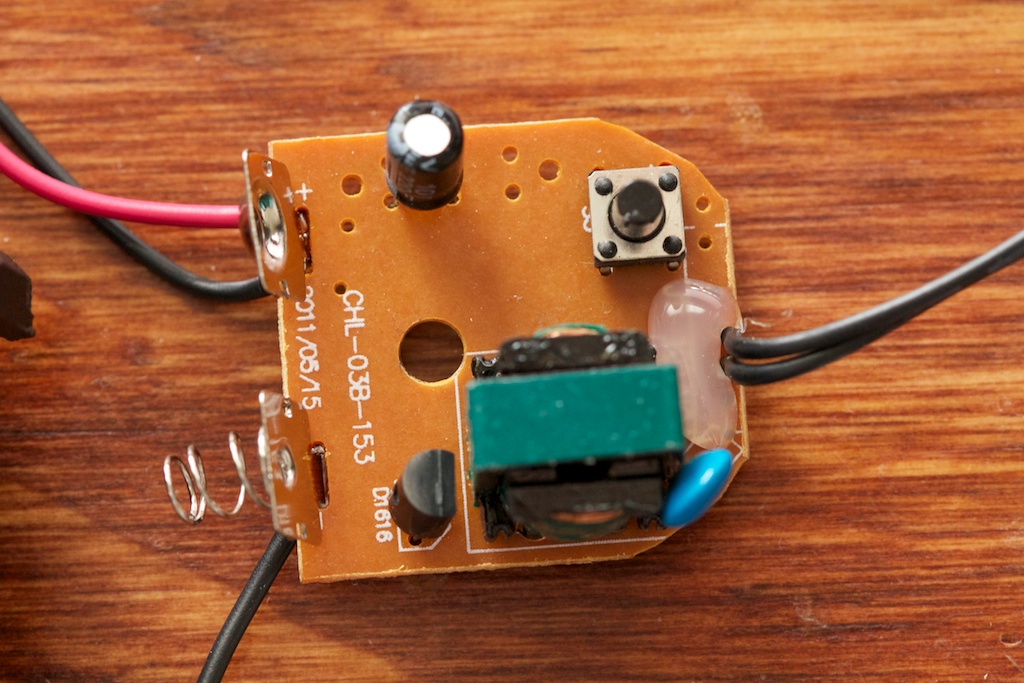
Each supply consisted of a simple 2-AA cell battery holder and a small PCB pictured here:
Like any voltage step-up device, there would need to be something to switch current on and off through some kind of transformer. My original thought was that the small micro-controller on board was responsible for setting the switching frequency, but I was mistaken.
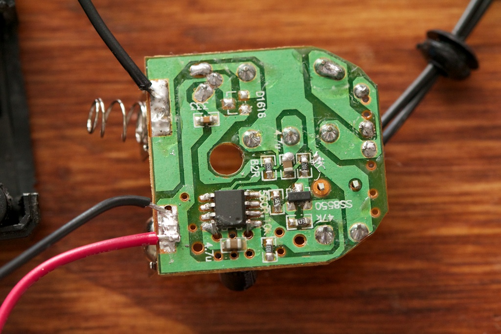
All the micro did was control the four different functions of the EL wire supplies: off, on, blink slow, blink fast (real awesome feature set guys!). The reason the circuit would not power up after a jolt is probably due to the micro controller browning out after a brief disconnection of the batteries.
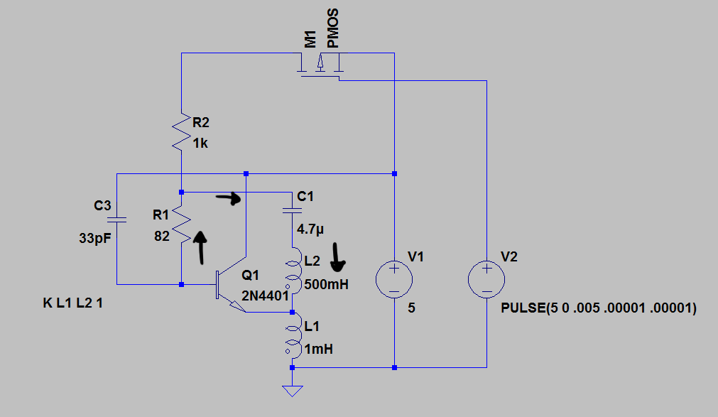
To turn on the EL wire, the micro simply had to pull down the gate of the PFET labelled SS8550. This FET would pass current to the rest of the circuit which as it turns out was an analog oscillator.
Things got a lot more complicated suddenly…
SPICE Up Your Life
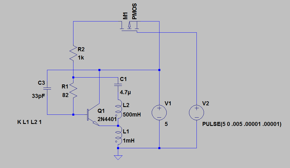
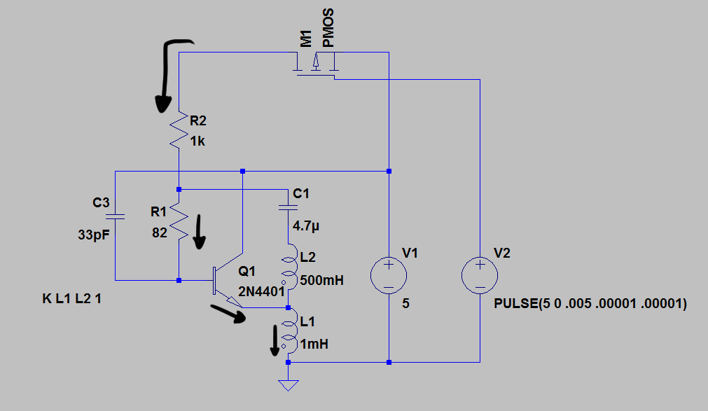
I’ve never been super awesome at purely analog circuits, so bear with me here. I quickly scribbled the circuit down in LTSpice which is a free circuit simulator made by Linear Technologies.
Bear in mind that the actual transistor used was a D1616, but I used the 2N4401 because it’s another generic NPN transistor that LTSpice already makes available. Also note that the D1616 has a rather unconventional pinout for a TO-92 package.
L1 and L2 make up half of a transformer. The other half (not pictured) is connected across the conductors of a strand of EL wire. The idea is that if this circuit can dump a lot of current through L1/L2, it will induce current through the secondary winding. Because the secondary winding has a much larger number of windings, its output will be at a much higher voltage.
To tell LTSpice that L1 and L2 are wrapped around the same inductor core (and thus share mutual inductance), I added the directive “K L1 L2 1”. This means that L1 and L2 are linked with zero leakage (100%). I learned a valuable lesson about LTSpice while doing this:
For about the first three hours of my head scratching, I was using a label as a SPICE directive and LTSpice was thus (justifiably) ignoring it.
Measuring Inductance
For my spice model, I simply guessed at the actual values of L1 and L2, but for fun, I decided to a attempt measuring them directly. More important than knowing the inductance per se is knowing the turns ratio of the transformer. The turns ratio is literally the ratio between the number of times the primary winding is wound around the inductor core to the number of times the secondary winding is. The winding ratio is directly proportional to the voltage ratio of the input to output.
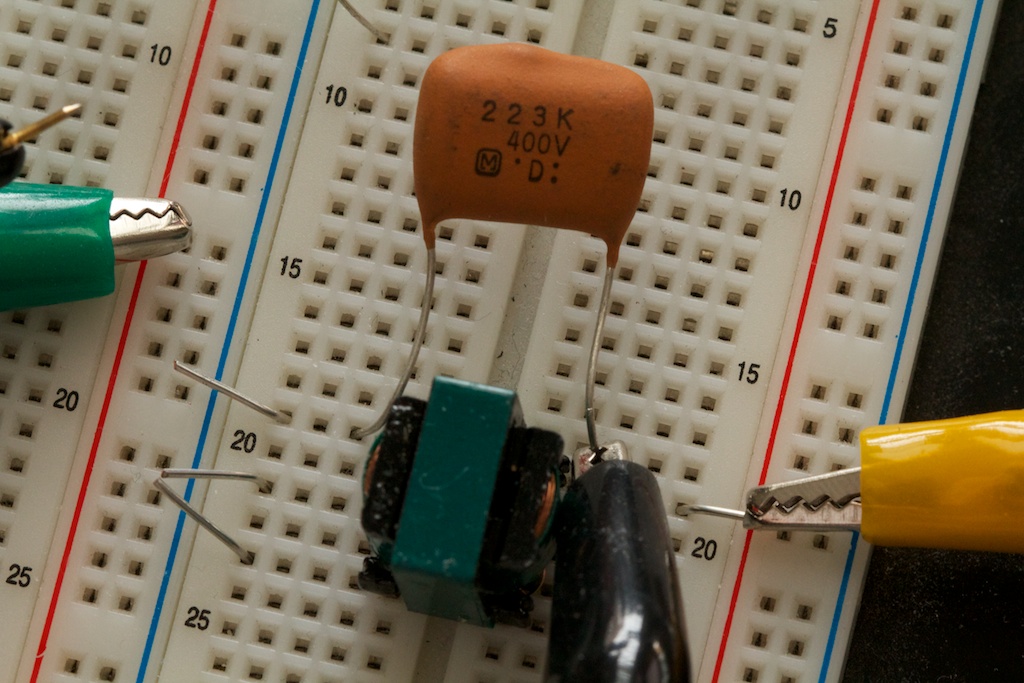
The turns ratio was easy to determine once I measured the inductance of the primary and secondary windings. To do this, I built a simple LC oscillator. By measuring the period of oscillation, I was able to approximate the inductance of my transformer.
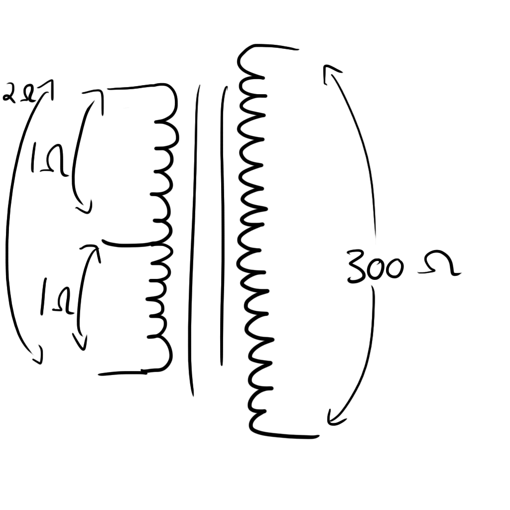
Determining the pinout of an inductor is a pretty easy task. Basically, although there is no resistor inside an inductor, the windings themselves will have some DC resistance simply because of how long and thin they are. I measured about 1ohm of resistance between the center and the ends of the center-tap primary winding and about 300 or so ohms across the secondary winding.
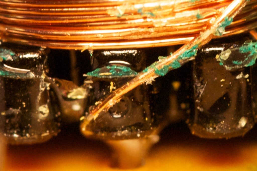
To further confirm, I took a look at the windings themselves. Here’s a photo of one of the non-center pins of the primary winding:
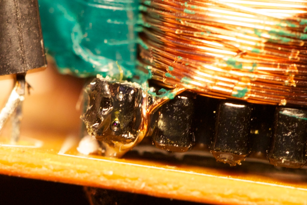
And here’s the center pin:
Notice the two wires?
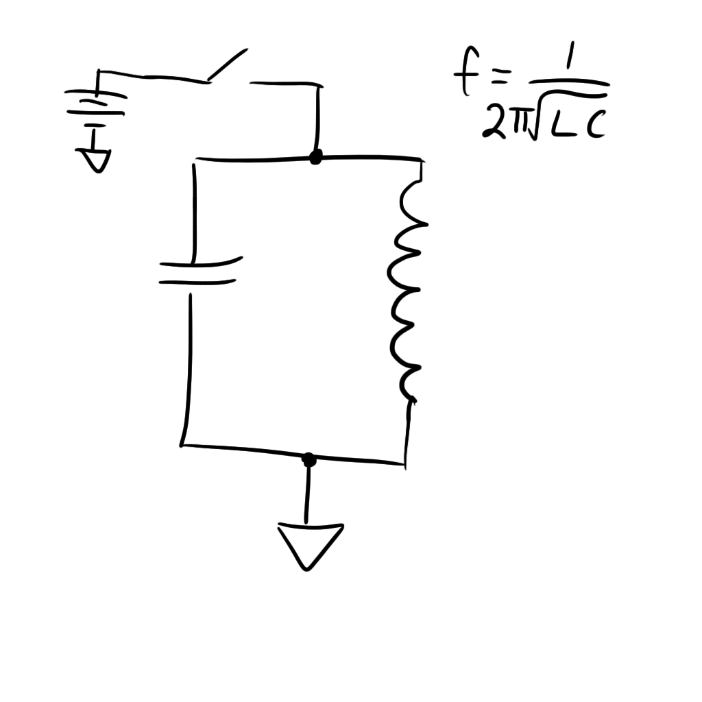
Here’s a simple schematic of my resonant circuit:
The formula pictured above is the formula for the resonant frequency of my LC filter. Basically, when the circuit is “flicked” (has a voltage source suddenly connected or disconnected) it will vibrate at that frequency. If that frequency could be measured, I could use the known value of C (23nF) to determine the value of L (inductance).
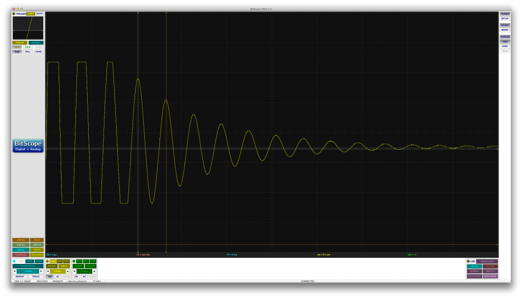
First, I measured the secondary winding of the transformer:
Disregarding that the voltage spike was large enough to peak out my oscilloscope, I measured the resonant frequency to be about 1.6kHz. This corresponds to approximately 450 milliHenries.
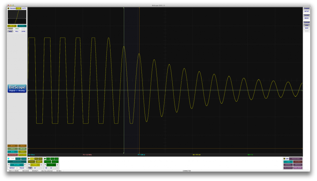
The primary winding has two parts (because it is center tapped). I first measured from the center tap to one of the ends:
This had a resonant frequency of about 35.7 kHz corresponding to about 903uH. Running the center tap to the other end produced similar results. Note that in my LTSpice model, I made L2 much much larger than L1. This is because LTSpice is very finicky about getting oscillators working, so I had to tweak the values to get the desired affect.
Remembering that a transformer is nothing more than two inductors wound around the same core, I had to determine the ratio of the inductances of the two windings. According to Wikipedia, the formula for the inductance of an air-wound inductor (one without a magnetic core) is as follows:
The only difference between an air-wound inductor and a magnetic core-wound inductor is the value of µo (the “Permeability of Space”). µo is a universal constant which is used when your inductor has a vacuum core. Otherwise, you use µ which is a ratio between the permeability of the core material and the fundamental value in a vacuum. As it turns out, µ for air is very close to µo. µ for ferrite cores is much much higher by design. µ is a chemical property of the core’s material and is much higher for magnetic material cores than air cores. Chemists are always trying to think up better materials with higher values of µ. If µ gets larger, everything else (including the size and weight) can go down.
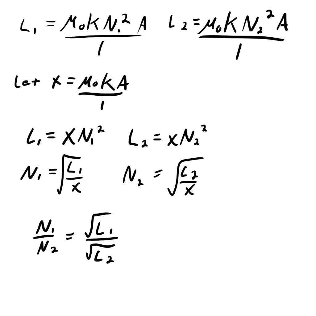
So, in this formula, A is the cross sectional area of the core, l is the length of the core, K is some special coefficient, and N is the number of windings. With the exception of N, all these values are properties of the inductor core and are therefore the same for both windings. So my winding ratio is as follows:
Using the values I determined, the winding ratio is approximately 1:22 which seems like a reasonable turns ratio. If my primary winding is clocking along at 3V or so (battery voltage), the secondary winding will be at around 75 volts.
Update: This is wrong! See details here.
Dissecting Their Circuit
So, returning to the power supply circuit, I set about understanding exactly how it works. I believe it’s some sort of blocking oscillator, but they might have made a few mistakes when designing it.
The oscillator is first turned on by pulling the gate of M1 low. This allows current to flow in through R2, the base of Q1, and eventually through L1 to ground:
Because L1 and L2 are coupled together, this ramping up of current through L1 should cause current to flow upwards through L2. You can think of it as L2 trying to “cancel out” the net change in current through the inductor.
Because we’re dealing with high-ish frequency stuff here, current passes right through C1. This current hits the base of Q1 and turns it on even harder acting as a sort of positive feedback loop.
Now, I’m not entirely certain what happens next, but my guess is that eventually the current through L1 reaches some kind of steady state. Because the current through the inductor is no longer changing, the current through L2 dies off. With less current supplying its base, Q1 begins to shut off.
As Q1 shuts off, current through L1 also starts to die down. L2 again tries to fight this change in current and starts inducing its own current downward to compensate.
With current being actively pulled away from its base, Q1 shuts off even harder producing yet another positive feedback loop. Once the current drops to zero, the whole process restarts.
As far as I know, R1 and C3 are only there to filter out any super high frequencies from hitting the base of Q1 and causing possible issues with EM radiation or whatever. Still seems odd for two reasons:
- C3 is tied to the +V rail when usually one would expect it to be tied to the negative rail. I suppose it really doesn’t matter either way and +V was definitely more convenient layout-wise.
- A 33pF cap and 82 ohm resistor make a filter with a cutoff frequency of 58.82MHz which seems insanely high to actually do anything productive. Oh well.
Despite my minimal grasp of the tenets of analog circuit design, there’s one thing I don’t like about this oscillator. They have an NPN transistor with the emitter tied to a floating line. This means that they can’t really guarantee that a positive voltage at the base will turn on the transistor if there is a large voltage drop across L1. For all I know, this might be the whole point, but it seems odd to me.
Update:
Their design is actually better than I thought. Details here.
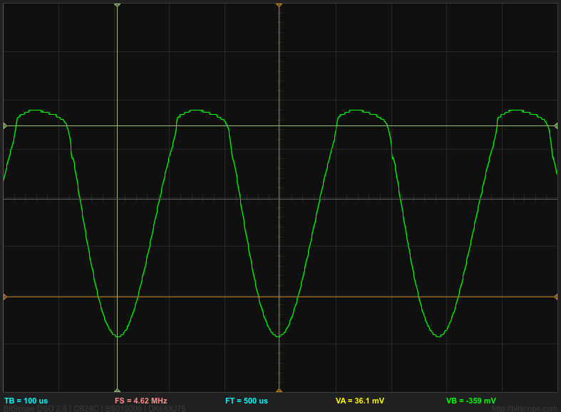
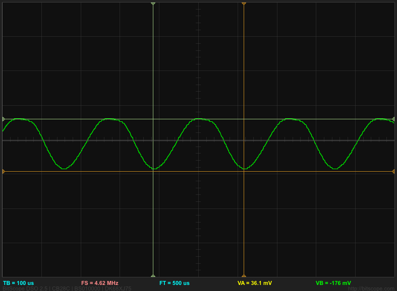
Firing their circuit up produces a fairly clean sine wave at the base of Q1 at about 3.3kHz:
Designing My Own
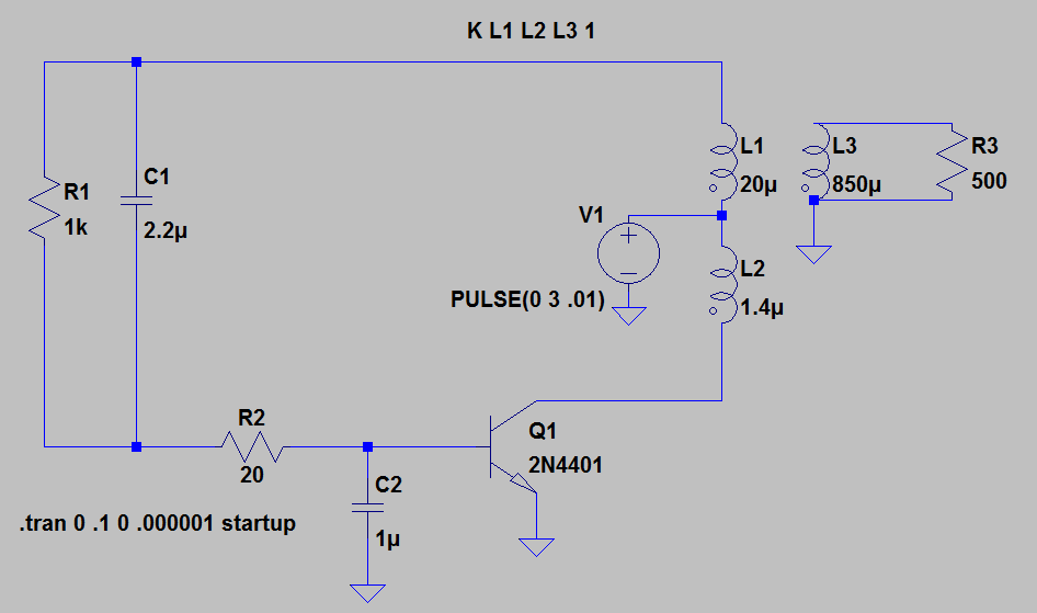
For my own power supply, I decided to change things around a little bit:
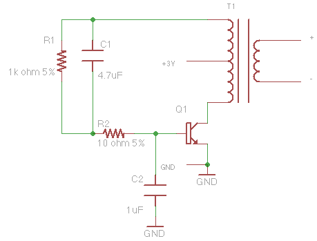
Again, I had to fiddle with the values a bit, but you get the idea. The function is similar to the original oscillator. As Q1 turns on, L2 induces current through L1 that turns it on harder and vice versa. The major difference is that the emitter of Q1 is tied to ground where it belongs.
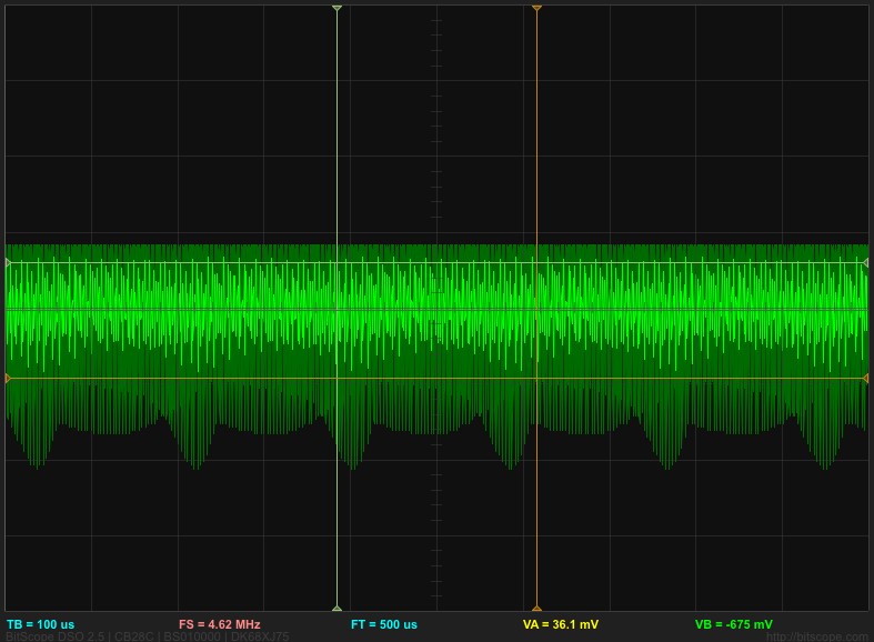
C2 and R2 were placed to solve an odd problem I was experiencing. For some reason, my new circuit worked fine without them last night, but when I tried it again this morning, I would get nothing but super high frequency (on the order of 520kHz) oscillation.
Pretty crazy right? Anyway, at such a high frequency, the EL wire wouldn’t light up. My guess is that at such a high frequency, the inductive action of the secondary winding prevented current from getting delivered to the load (inductors look like open circuits to high frequencies, remember?). Again, I don’t know exactly what was going on, but adding that RC pair tidied things up nicely:
The RC pair that I used (10ohm, 1uF) had a cutoff frequency of 16kHz, so this prevented any higher order harmonics from showing up and getting amplified.
Here’s a schematic for my oscillator:
The cool part is that the whole circuit is smaller than the inductor itself, so it makes for a pretty compact design:
Efficiency
Given that I didn’t exactly design this circuit so much as I guessed and checked, I was interested in finding out exactly how efficient it was. Firstly, I compared the brightness of my circuit to the brightness provided by one of the original power supplies:
Looks about the same to me! This was for two sections of the same type of wire that were approximately the same length. Doing a comparison like this isn’t exactly fair though because it’s possible that the electric fields from the brighter wire is actually lighting up the dimmer one. To be sure, I took them into a dark closet to separate them and see if I could tell them apart. They really appeared to be the same brightness.
I then set about recording the current draw from the batteries of each circuit. The original circuit clocked in at about 116mA of current while my new one only drew 58mA! That’s close to exactly half the current draw! Furthermore, my circuit is smaller and doesn’t whine quite so loudly.
I really feel kind of odd about that. Was the Chinese circuit really that bad or did I just completely luck out with my circuit design?
Update:
Conclusion
Well, that was a lot more long winded than I was originally planning, but I’ve been wanting to better understand EL wire since I first bought the stuff, and although I don’t fully understand oscillators, I’m definitely better off than I started.
I’ll be doing some more stuff with EL wire in the future including making a more compact (and more efficient!) power supply for my shutter shades. Stay tuned.
Continue this story here.







Your projects are interesting. I can’t wait to see a more compact power supply for the shutter shades. I am actually the vice president of ASME at James Madison University and we are using design along with what some other people have done as the base for our design and we hope to sell them for fundraising.
I’m flattered!
Let me know if you need anything about the design clarified.
Hello! Wondering how ‘loud’ the inverter on your mod is? Were you able to make it any quieter? I have some of these inverters and they make the most annoying noise…some muffling helps, but I feel that is not the right way to approach the noise issue. Any ideas would be very appreciated!
I can tell you that after modifying the supplies like this, they became a LOT quieter. You can still hear them if you try, but it’s a lot less obnoxious than the alternative. I’m not entirely sure why this is, but I think it has something to do with making all of the currents involved a lot smaller and thus lowering the “singing” that comes out of the transformer from magnetically actuated vibrations.
Ok, that is good to know! I have read of all sorts of attempts to silence the whine, including casting the part in resin. Seems the best way is to redesign the circuit or modify as you have. Here is the link to a discussion on adafruit: http://forums.adafruit.com/viewtopic.php?f=8&t=18811&sid=f8d98fae2fa1ed3b370bec779debfea6&start=15
Great blog by the way, very nice approach to documenting the projects!
Pingback: Revisiting the EL Panel and the True Meaning of RMS | ch00ftech Industries
Pingback: I Should Give China More Credit | ch00ftech Industries
Soo, you said you design that circuit?
http://www.youtube.com/watch?v=AcXHx5ikjM4
Min 6:10
There only a number of different topologies for blocking oscillators. I’m not surprised that mine is similar to hers. More details on different topologies here: https://ch00ftech.com/2012/08/17/i-should-give-china-more-credit/
Which IC used in this circuit??
Plz rply about it
And if possible then send detail about transformer!!
I’m not sure which IC they used. It’s probably a micro controller with custom firmware or at least an application specific part. My reproduction of the design only needed a single transistor.
hi
Do you have any suggestion for the IC used in this circuit?
You know, i want to do a reverse engineering of the circuit.
thanks
l
EL (ElectroLuminicent) wire. EL != The.
Do you have any recommendations for a similar inductor to replicate the circuit above? Mainly some small one as I’d like to to have it as small as possible for lighting a portable handheld system. Thanks.
You ruined my day! C3 is not 33pF. It is 33nF. I lost many hours checking what is going on…