Today I decided to take on this bad boy:
Intro
If you’ve been reading my blog regularly, you’ve probably already seen this thing in my icebreaker post. The toy functions as a portable low-resolution scanner that can scan and save a number of images and then reproduce them using persistence of vision.
In the icebreaker, I ripped off how they handled measuring the oscillation-rate to produce the persistence of vision. I could do this without even opening the case. For a future project, I wanted to find out how they managed the scanning function. That’s a little more in depth.
My assumption was that they were scanning using the LED-as-a-sensor trick that I wrote about in this post. The only problem was that with my implementation, the trick requires twice as many micro-controller pins as LEDs. When you get up to 32 LEDs, this gets kind of ridiculous. I wanted to see how they did it.
A starting question
Before getting into the details of the circuit, something has always bothered me about this thing. It has 32 LEDs on its front, and can produce images with 32 pixels of height. As you scan, you can see LEDs illuminate in order. My assumption was always that one LED would turn into a sensor and one or two neighboring LEDs would illuminate and bounce light off the scanned page into the detector. This means that the micro just has to store the values picked up from each LED and then reproduce them when the device is in playback mode.
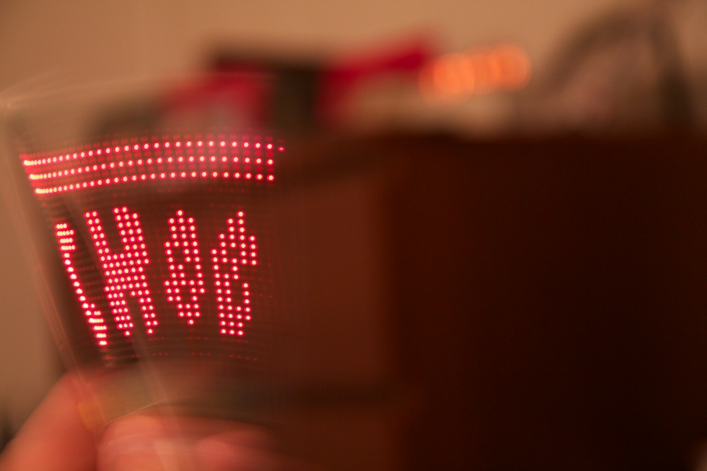
Using my SLR, I took a 1/1250s photo exposure of the scanning mode in action, and came up with this:
So that confirms that only one LED is lighting at a time. I guess the two neighboring ones are being used as sensors.
The only problem is that it seems like not every LED is being used as a sensor. Take a look at this video.
From here on out, the LEDs being used as sensors will be called “sensors” and the LEDs used as lights will be called “lights”. This only applies in the context of scanning. During reproduction, all LEDs are “lights”.
I figured there had to be some kind of algorithm running inside the micro that would interpolate the pixels between rows and turn a 16 pixel high image into a 32 pixel high image. To test this, I came up with a little experiment.
I used a marker to cover up three of the sensors and did a quick scan. I came up with this:
You can see the three sensors are lighting up (dimly) behind their black marker mask, and the lights around them are also lighting up. This means that the firmware picked up that three of the sensors in a row were coming back black, so the lights between them must also be black.
Now, it is still possible that the LEDs swap jobs for a very very short period of time (lights become sensors, sensors become lights). The results of this experiment could be explained by the fact that the sensors (now being used as lights) are covered up so that the lights (now being used as sensors) have no light to detect. To test this theory, I ran the experiment again supplying light from an external source to the group of covered sensors. I came up with the same results.
So, there is some algorithm that determines the values for the lights using the data from the neighboring sensors.
The circuit
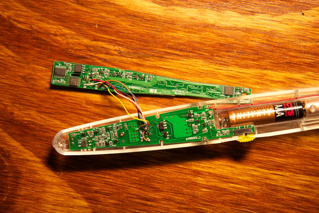
The circuit is split into two boards.
In this image, the bottom board deals mostly with power regulation and the oscillation sensing unit. The top board is where all the brains are. There are four ICs on the top board:
- 74LV4051 – A standard 8 port analog multiplexer. A multiplexer means that the device has no means to illuminate two LEDs simultaneously. They must be pulsed in turn very quickly.
- 24LC16 – A 16K EEPROM that is likely used to store the images after they are scanned (the device can store up to six different images and retains them through power loss).
- “1AP G0K1” – I was unable to find out what kind of IC this was, but I think it’s safe to assume that it’s some kind of micro controller.
So. The LEDs are multiplexed. Interesting. This is a little worrying for my future endeavors because blinking LEDs that quickly requires a pretty hefty micro controller or an FPGA. The former is expensive, and the latter I’ve never worked with.
EDIT: Reddit user answerguru pointed out that I really don’t need a very powerful micro controller to do this. I guess I was picturing in my mind those LED marquee displays you always see in the lunch line which always seem to have a distorted image whenever you dart your eyes around. Waving one of those around like this toy would cause a lot of issues. My concern is being able to flash the LEDs in quick enough succession such that the vertical rows still look like straight lines. After reading answerguru’s comment and running the numbers, I realized that this shouldn’t be a problem. If the gadget is moving at 3 feet per second and I want less than a millimeter’s distortion between any two LEDs, I would need to blink the entire row in just under 1ms which is eons for a micro. Thanks for the tip answerguru!
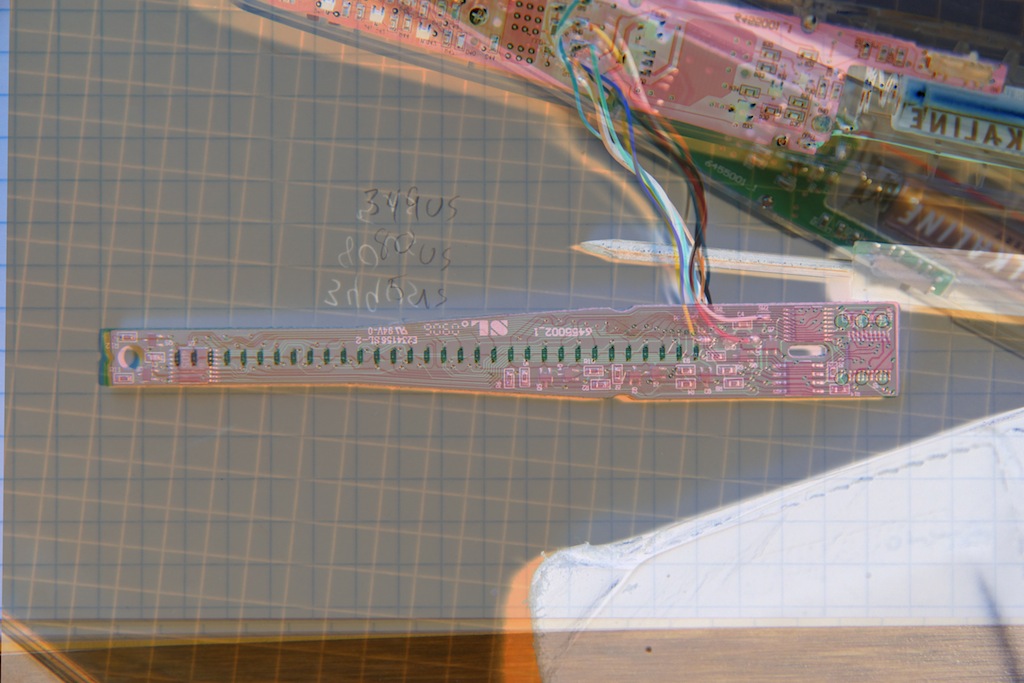
Either way, I took another photo of the back, and loaded them up in Photoshop as two separate layers. After mirroring the back and inverting its colors to add contrast, I was able to align them like this:
Playback
My first task was to figure out how images are being displayed on the LEDs. I started by using the paint brush tool in Photoshop to color code exactly which LED is connected to what. It looked like half of the LEDs were connected to the first multiplexer and half to the second. Here are the connections for the first one:
It’s hard to make out, but there are little dots on the pins of the leftmost IC which are color coded to the LEDs. And here’s the second:
As you can see, each pin from a multiplexer connects to two LED anodes. This makes sense; there are 16 ports available between the two multiplexers and 32 LEDs in total. This likely means that control for the LED cathodes is split so that only one of those two LEDs can be illuminated at a time.
Looking at the cathodes, I noticed a pattern where it seemed that every other anode was connected together. You can see that in this image stenciled in white and gray (I only bothered to do half of the LEDs, the other half follow a similar pattern but on two different lines).
The anode lines converge on two transistor circuits shown here:
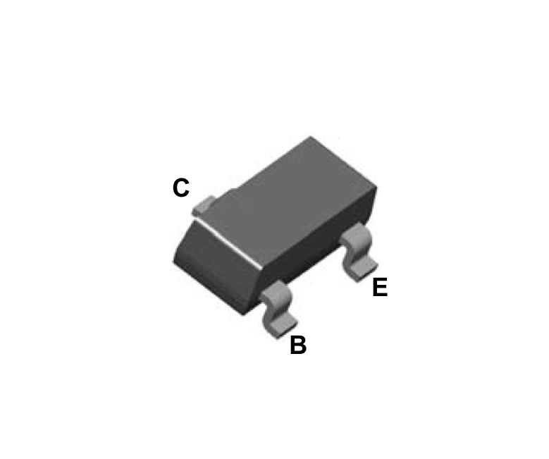
I had to figure out what the transistors were. They were labeled with just “24” and “54” which turned up nothing on Google. Assuming that they were BJTs and used the common pin ordering for BJTs in a SOT-23 package:
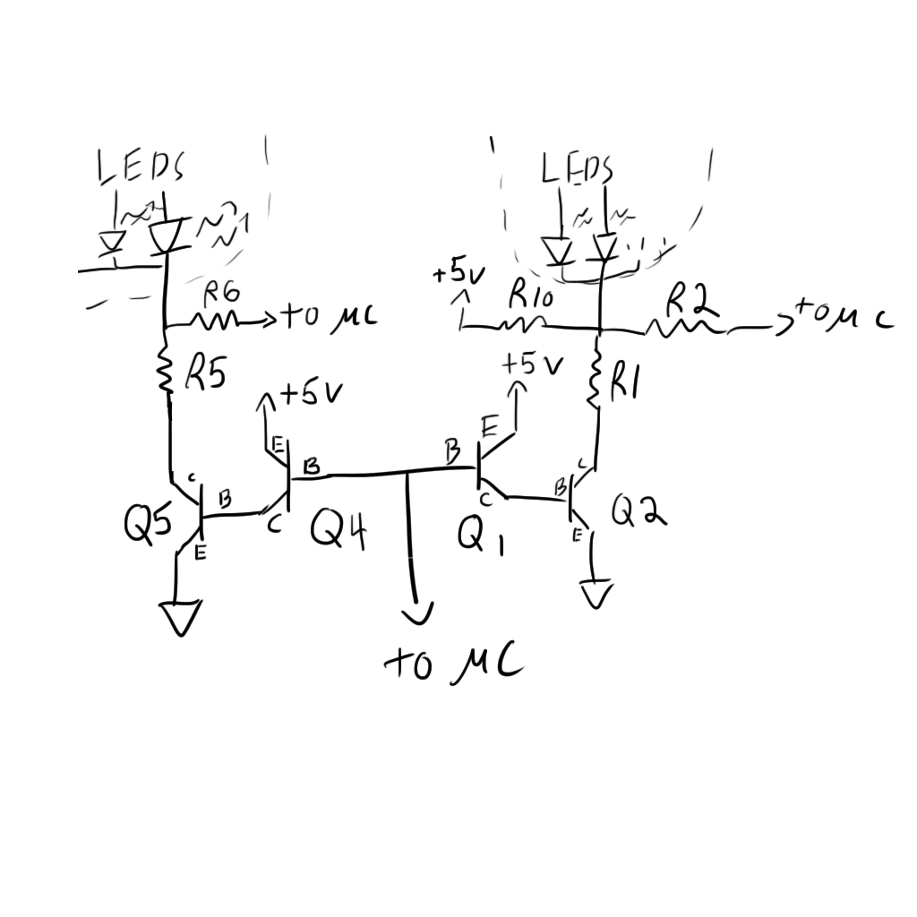
I was able to re-draw this part of the circuit as follows:
Now it was just a task of figuring out which transistors were PNP and which were NPN. I noticed that during normal operation (with an LED lit), the emitter and collector of Q4 were high with the base pulled low. That would seem to imply that Q4 was a PNP transistor: Pulling current from the emitter to the base caused current to flow from the emitter to the collector. Similarly, the emitter and collector of Q5 were low as the base was high. This would imply that Q5 is an NPN. Q4 was marked with “54” and Q5 with “24” so I guess all the 54s are PNP and all the 24s are NPN. Adding the appropriate markings to my schematic produces this:
It’s worth noting that R1 and R5 are 90 ohm resistors which means that these LEDs are probably being run a little above spec. Assuming a Vf of 2v (typical for red LEDs), that gives you a current of 33mA! This is acceptable though considering how the LEDs are all being driven at a very low duty cycle.
It’s not quite clear what the connections through R2 and R6 do. My first guess was that that’s how the micro controller reads the voltage off the high side of the LEDs as it drops (assuming they’re using the same method I used for the LDDs article), but as I found out later, that’s not the case. They aren’t unique connections either. The line coming from R2 also connects to R4 which serves a similar purpose in one of the other low-side drivers.
So, one issue I noticed is that all four of the low side drive circuits (these two and the two driving the rest of the LEDs) are all controlled by the same line coming from the micro controller. This really bothered me for quite a while because as I said earlier, in order to have two LED anodes on the same multiplexer port, there needs to be some way to drive the cathodes independently. Well, it turns out that the other two circuits aren’t the same as the first two. They look like this:

Where one of them includes the resistor to 5v like before. So this solves that problem. When the signal line from the micro controller is low, the first two ports are off and the second two ports are on. When the signal is high, the opposite happens. This prevents the micro from being able to control two LEDs simultaneously. It interesting to note that this method isn’t perfect as there will be some crossover when both of the LED sinks are active. If you darken the room and look closely, you can often see a slight ghosting effect as the image from the top of the stick is repeated to the bottom very dimly. This isn’t noticeable though unless your image exists primarily in one half.
Scanning
Now scanning on these LEDs is a lot more complicated. The whole method depends on the touchy-feely process of running an LED in reverse bias. LEDs aren’t really meant to do this, so the LED manufacturers aren’t going to make it super easy. This requires some gentle massaging on the part of the engineer designing the circuit. Without access to their test data and data sheets, it makes it very difficult to tell exactly what is going on.
As I said before, the high side of each LED bank is an an analog multiplexer. The common pin of this mux has a PNP transistor dropping current into it and by extension into the LEDs. One of the muxes also has an additional three terminal transistor device seen here as Q9.
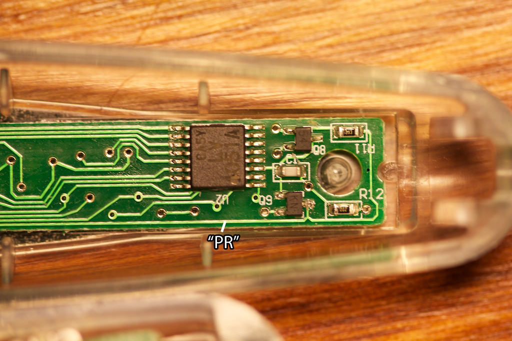
Also indicated here is the “PR” trace. This trace runs straight to the micro and also on to the second board. I’m not certain what the “PR” stands for, but I’m pretty sure that this is an analog line that feeds into an onboard ADC on the micro. This would explain why it’s connected to the other board; it’s used to measure the voltage off the proximity sensor that the device is using as a cheap accelerometer as I did in the icebreaker.
Here’s a simplified doodle of this part of the circuit:
During scanning operation, the BJT’s base is pulled high, turning it off.
Now back to that Q9 device. It’s not marked 54 or 24 like the other BJTs and my guess is that it’s some kind of FET. This would make sense because the gate of a FET would provide a very high impedance allowing the small amount of current coming from the LEDs to charge the capacitor and raise the cap voltage. The rising voltage on the gate of the FET would turn it on or off appropriately and allow a nice buffered signal to go the the ADC of the micro along the “PR” line. Here’s a trace of the PR line during scanning operation:
This is the device scanning a number of LEDs. The FET device appears to work as an inverter (pulling down the 33k resistor) so the sloping voltage drop you’re seeing here is actually the voltage rising on the capacitor. Two things are interesting about this picture:
- The micro appears to spend an equal amount of time measuring each LED. This is how I realized that it had to have an ADC (as opposed to measuring the varying amount of time it would take the cap to charge to a fixed voltage like I did in my LDD).
- Some LEDs charge the cap more than others. This makes sense because for this trace I was scanning a drawing that I did in Sharpie on white paper.
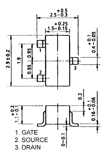
I marked the Source, Drain, and Gate in the above schematic following the standard SOT-23 ordering:
Now, unlike the BJTs, searching for a SOT-23 device marked with “KN” did turn up a result. I found the 2SJ305 which is a P-type FET. This was troubling to hear. Typically for a P-FET, the source is tied to the high voltage rail. With the source tied to ground, it would be impossible get a negative Vgs to even turn the FET on!
Well, I really worked on this problem for a while. It’s possible, that because the source is tied to ground through the 2k resistor that the source could float up a bit and allow a negative Vgs, and it was that much more believable because I figured that the designers would have been pulling some serious black magic to get this gadget to work anyway.
Well, I got frustrated and decided to ask the minds on the /r/ECE subreddit. I got some pretty awesome responses. They pointed out that it’s completely plausible that the device is actually an N-type MOSFET as often times multiple components will share the same labels (and even be mis-labeled entirely!).
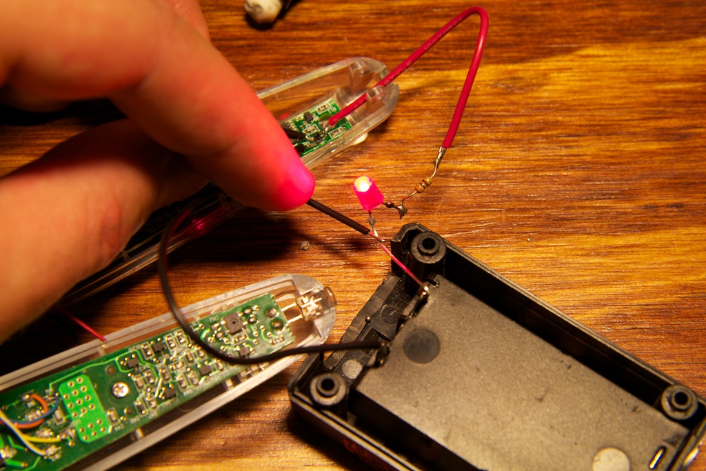
Just to be sure, I ran a little experiment with this circuit:
The gate was attached to a free piece of wire that I could connect to various parts of the circuit. I soldered the circuit right on to the mystery FET straight on the board. This was easier than desoldering it, and assuming power was disconnected to the board, it would likely be no different.
Here are my results:
This is it with the gate floating (I noticed the same results when I tied it to ground, so the analog mux must be grounding it). The LED is on, but only slightly.
BOOM! When I attached the gate to the positive rail, the LED got super bright. This means that my suspicions were correct. It’s not a P-FET at all, but rather an N-FET with the source tied to the low rail like it’s supposed to be.
Putting it all together
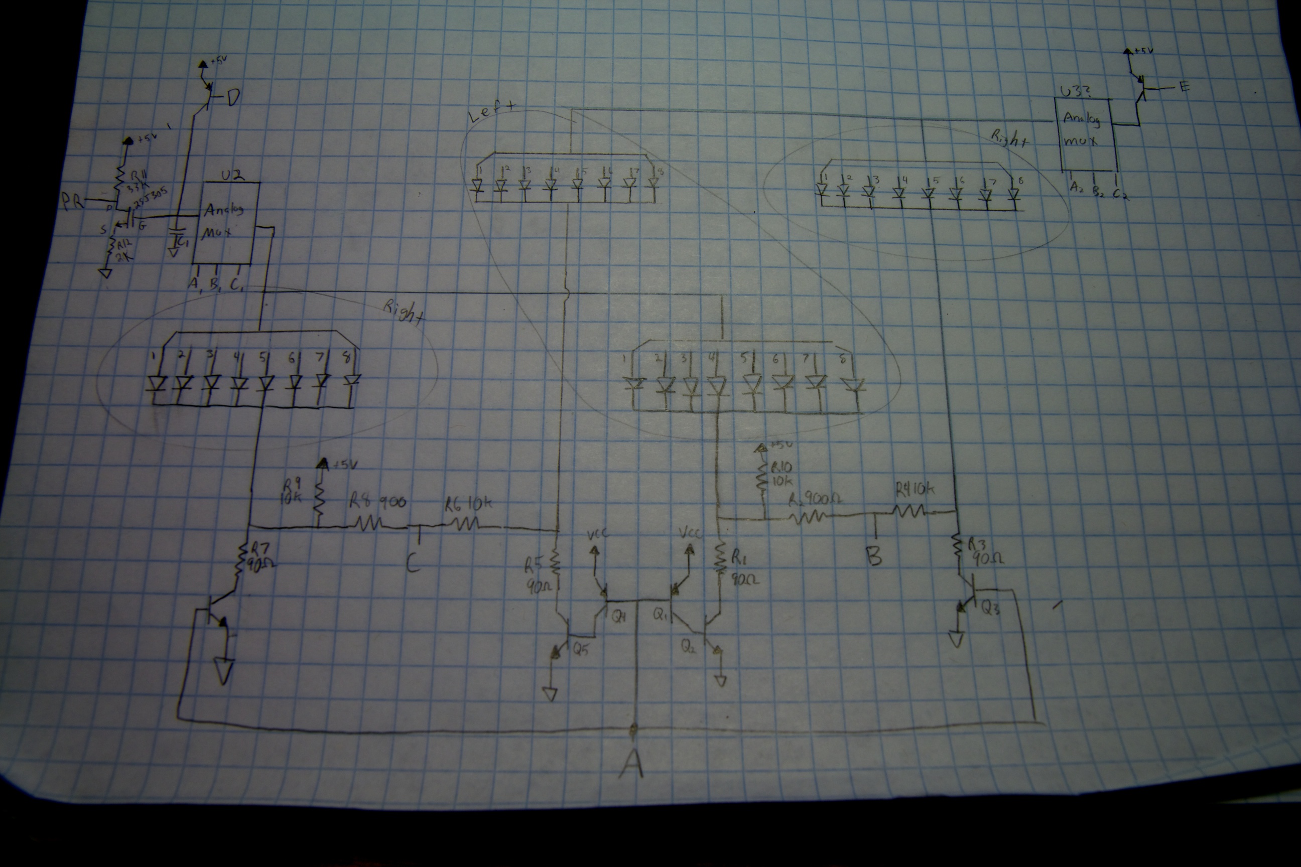
All together, my circuit now looks like this:
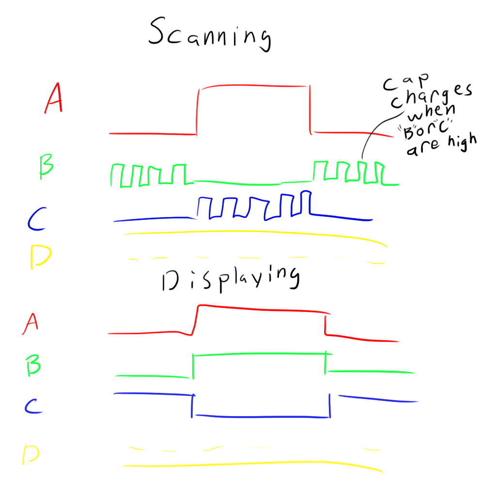
And here’s a timing diagram doodle to help out:
For scanning, the LEDs are arranged in such a way that when the current sink is active to turn on the necessary light, the current sink for the adjacent sensor must also be activated. B and C appear to fight that current sink and pull the LED cathodes high but only to about .5V. I’m not too sure what the purpose of this is because there’s nothing stopping the circuit from having the adjacent lights and sensors on two different current sinks. Perhaps if they were able to pull it up to 5V, the LEDs would conduct too much current too quickly or something?
I think in the context of displaying on the LEDs, B and C just tag along with A to help pull down the LED cathodes that much more.
Remaining questions (and answers)
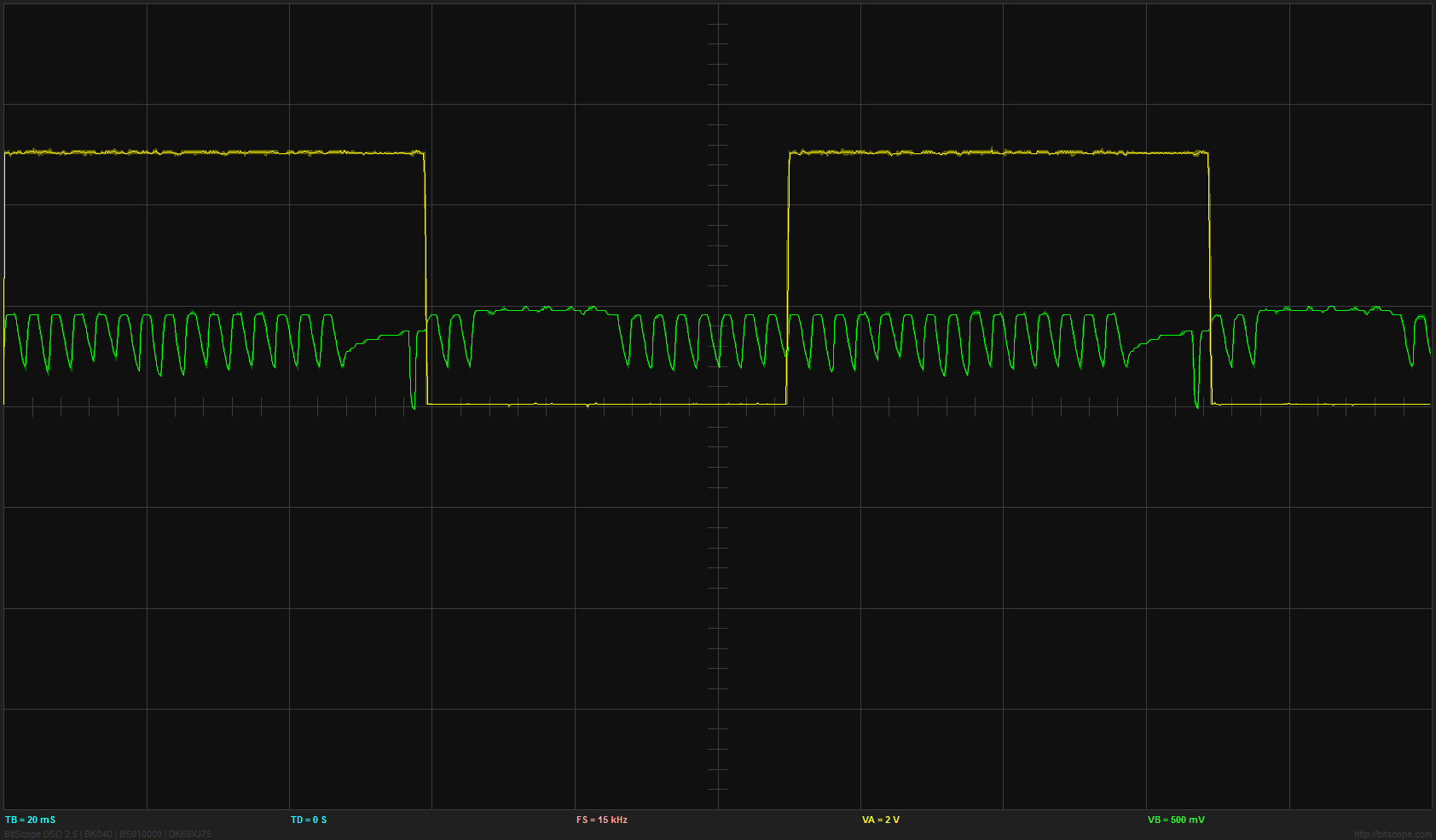
My biggest remaining question was exactly what purpose R9 and R10 serve. They appeared to be some kind of pull up resistors, but they seemed to be doing a lot more than that. This is a scope trace of A (yellow) and the PR line (green) (different voltage scales):
So you can see that the cap is being charged and discharged both as A is high and low. Here’s the same trace with R10 removed:
Obviously, it’s totally screwed up. Here’s the really weird part. When I removed R10, I noticed that this seemed to break the scanning functionality of the LEDs labeled as “Right” on my schematic. Also, you can see that the PR line doesn’t oscillate when A is high. That means that as C is oscillating, the PR line does nothing.
The weird part is that R10 isn’t even close to C or the “Right” LEDs!
Well, it wasn’t until I had it all drawn out that I realized exactly what was going on. I had forgotten that this gadget is multiplexing the LEDs so that while one LED is being used as a sensor, there is another one joined at the anode:
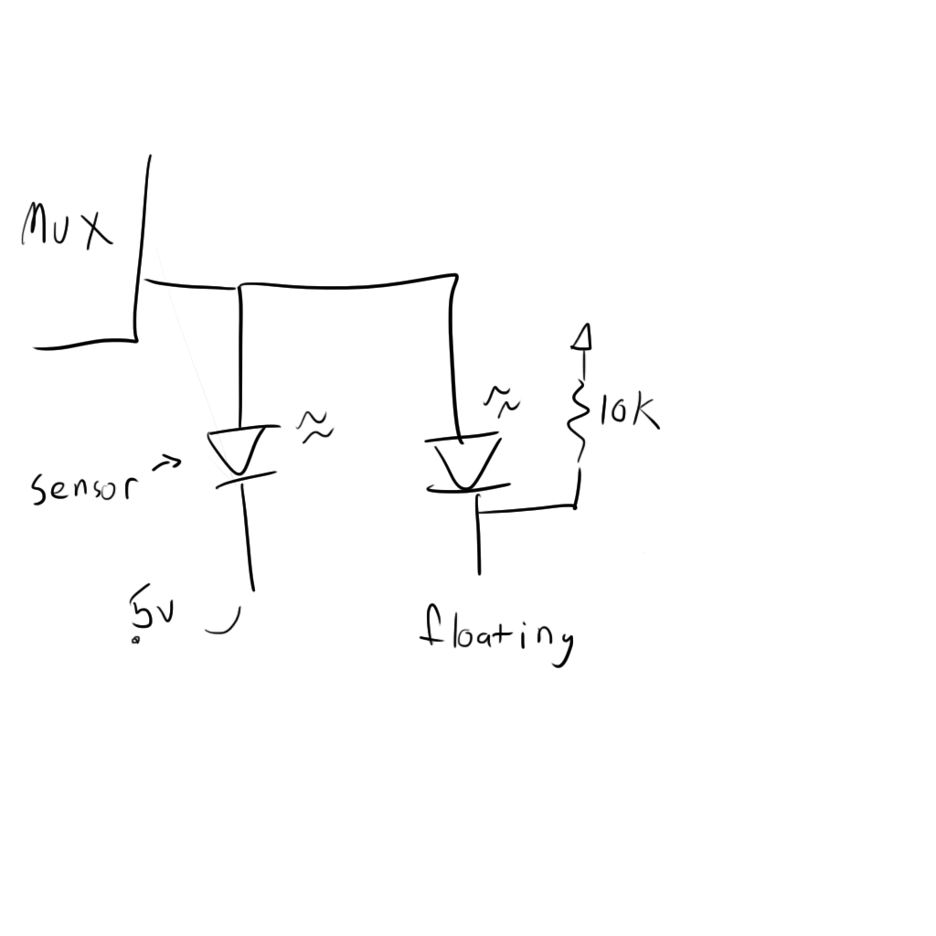 If that 10k resistor wasn’t there, the second LED would suck all of the reverse current out of the mux and prevent the capacitor from charging! With this configuration, when the mux is measuring an LED, it’s also measuring its twin, but the assumption is that the twin isn’t very well illuminated, so the reverse current will be negligible.
Now the only thing I’m left wondering about is what R4 and R6 do. They lightly attach the C and B lines to the LED light sinks. My guess is that the designer just wanted to keep the cathodes of the LEDs from floating when the sink was turned off, and added that in there. Removing R6 didn’t have any appreciable effect on device function.
Conclusion
So, I still don’t know exactly what’s going on inside the micro controller, but it’s pretty easy to guess that it’s taking analog readings from all of the LEDs, using their values to determine some black vs. white threshold, and storing the values in its EEPROM to be displayed on the LEDs.
There is still more to the circuit (power stages, etc), but I covered all of the real magic in this review. I’m planning on implementing a similar technique in a product I will be developing, so this definitely provides an awesome head start.
This is my first time ever trying to reverse engineer a product, and I’m really impressed with myself. I certainly wasn’t expecting to get such a complete picture with so little information at my disposal. If I find another product that is similarly cool, I’ll be sure to do another one of these write-ups!
I hope you enjoyed it!











So what does this all mean for the toy owners now?
Can I download torrents using this toy now?
Can I play doom on it?
Can I ssh into my box from half way around the World now?
Can I play NES games on it?
Just kidding man. Nice work 🙂 I’ll go through everything when I have time.
Working on a Linux distro. It’s just a pain in the ass to keep waving it through the installer. 😉
I have seen this toy in action before. Where did you get it? I want one!
I bought it on Think Geek, but it was over four years ago. I don’t know if they still offer it. The product is called a “LighTalk LED Scanner”. It ran me about $40.
Pingback: Longboard Wheel Display | ch00ftech Industries
Pingback: Getting Itty Bitty With The Ice Breaker 2.0 | ch00ftech Industries
Pingback: PrintSnap Instant Camera | ch00ftech Industries