Alright, so I had some post-publication weirdness following my last post, and it took me a few days to figure out exactly what was up, but I think I finally have all the details, and I learned a lot in the process.
The Issue
I noticed some weirdness towards the end of writing my 8,000+ behemoth of a post last week. For those of you just checking in, I built a simple Class D amplifier to provide an EL panel with a +/- 120V square wave.
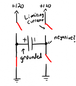
A Class D is basically an H-bridge attached to a DC/DC boost converter. Here’s the schematic of my H-bridge along with the output bypass capacitance of my DC/DC flyback (boost) converter on the left. The two tabs in the middle connect to my EL panel:
I spent most of the post designing my boost converter based on my expected load. My load was an EL panel which I measured with an LCR meter and got the following:
| Testing Frequency | Capacitance | Series Resistance |
| 100Hz | 66.8nF | 450k
|
| 1kHz | 62nF | 56k
|
| 10kHz | 57.9nF | 2.7k
|
| 100kHz | 42.2nF | 66
|
Based on some rudimentary research, I had assumed that an EL panel could be modeled as a resistor and capacitor in series. The resistance would drop as the frequency increased, but because I was planning on driving no faster than 1kHz, my load would primarily be a 56k
![]()
resistance or greater.
I used 56k
![]()
as my desired load and did all my component sizing based on driving that steady load at 120VDC. Once I finally put everything together though, I noticed that my positive rail wasn’t doing a very good job maintaining that 120V:
This is the positive rail stepped down by
![]()
by a voltage divider (my scope can’t take a 120V input), so my voltage was actually sagging from 120V all the way down to 45V. That’s 75V of ripple!
Now, I had some explanation for this. My flyback converter was controlled by a special chip that tries to maintain the output voltage by controlling the duty cycle going into the flyback. It’s possible that the flyback controller was simply not anticipating the sudden increase in load on the rail and therefore was unprepared when it hit. It was essentially going from an infinite resistance (fully charged capacitor) where it had probably dropped the duty cycle close to zero to a 56k
![]()
resistance where current would actually be flowing. Or so I thought.
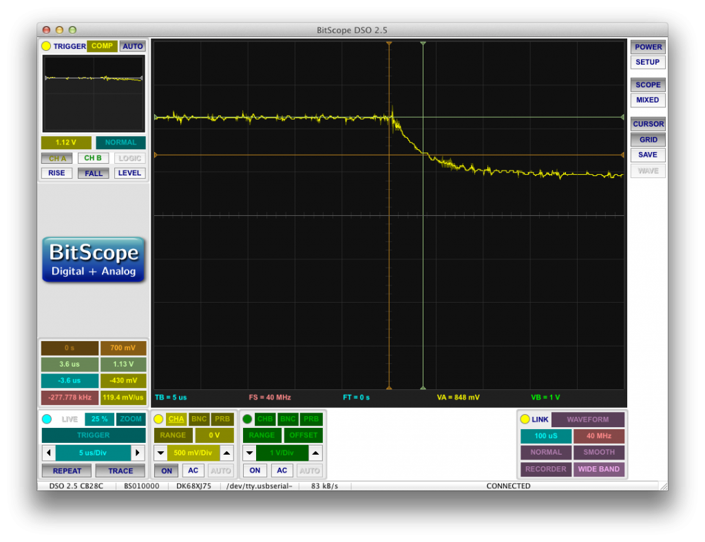
Trying to confirm this theory, I took some measurements of the slope of the voltage drop figuring that because the flyback was basically shut off at this point, the only thing supplying current to the load were the bypass capacitors on the rail (C16, C17, C20 above).
Now, when I originally published the post, I found the initial voltage drop to be consistent with a 3.6mA load which is about on par with what I was expecting for a 56k
![]()
load.
It was only after publishing did I realize that I was measuring with a voltage divider and forgot to convert back to real Volts! This means that I wasn’t drawing 3.6mA, I was drawing 360mA! This was completely impossible with a 56k
![]()
load!
So what the hell is going on here and how can I fix it?
The Quick Solution
So, I remarked in the last post that this problem could easily be solved by just adding more bypass capacitance. As it turns out this solution is correct. After adding a huge 4.7
![]()
F 160V capacitor in parallel with the measly .03
![]()
F I already had, not only did I virtually remove the voltage ripple, but I also reduced the audible noise that the converter produces by a LOT. See?
So it would appear from the video that a steadier rail actually makes the EL panel dimmer. It looks like in this situation, my panel benefits more from a higher voltage peak than from a steadier rail. My larger capacitor is averaging the ripple, and at this frequency, my power supply can’t keep up with the current draw. The average voltage is actually much lower than the peak.
This leaves me with two options. I can either leave the power supply how it is and accept a slightly dimmer panel, or I can redesign it from the ground up to make it better. I might end up doing both, but that’s a project for the future. For the present, my only concern is better understanding the problem.
Understanding the Problem
This issue all starts with my completely incorrect model of my EL panel.
My Completely Incorrect Model of My EL Panel
When I originally wrote my post, my model looked something like this:
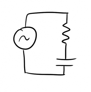
I had measured the R and C with the LCR meter, and was convinced that I was right figuring that the energy dissipated in the resistor was the energy you see as light.
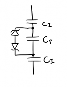
After doing some more extensive research, I found some other sources like this paper on EL displays which had a very different model:
The idea is that an EL panel consists of three parts. There is a phosphorescent material in the middle, and it’s sandwiched between two layers of insulator. At low voltage, each layer acts like a capacitor in series with the others. This is probably the capacitance I was reading with the LCR meter. At higher voltages though, the voltage across the phosphor layer gets large enough to allow for “electron transport” where the electrons of the phosphor layer get excited and move around.
In our model, we show this by including the two zener diodes across the phosphor layer. Zener diodes are like regular diodes that freely carry charge in one direction, but they can also carry charge in the opposite direction once the voltage across them gets large enough. When this threshold is reached in this model, one of the Zeners will turn on and the pair will short out the center capacitor increasing the overall capacitance of the system (remember your series rules for adding series capacitance). The energy expended by the current traveling through this zener is the energy that you see as light.
This also explains why you must drive EL wire in AC. If you were to just drive it in switched DC, the charge that moved through the zener in one direction would never be able to move back. Over time, it would leak through the capacitor, but this is very bad for the panel and will shorten its life.
The paper goes on to explain how if you plot the stored charge vs. voltage plot of an EL panel, you can see a hysteresis that indicates your panel’s energy output. I was really hoping to produce a plot like this with my panel, but I do not have the equipment to do so, so if you’re interested, take a look at the paper.
The real take home message here is that an EL panel is not a linear circuit component; its series resistance and capacitance change drastically as voltage changes. The 56k
![]()
that I measured at low voltage is probably much larger than the actual resistance that the panel is presenting at 120V.
So, my actual resistance is a lot lower, that explains the enormous current draw when the panel’s polarity is switched. Something still wasn’t adding up though. Something was funny about my voltage waveform.
Driving Capacitors
So one thing that’s funny about this circuit is that I’m driving a capacitive load with an H-bridge. That means that when my H-bridge polarity changes, my boost converter must provide current just to bring the load’s potential back to zero before actually charging it up the other way around.
This is weird because left to its own devices, a charged capacitor will discharge through a passive load like a resistor. Ideally, an H-bridge would connect both sides of a charged cap to ground to allow the charge to dissipate passively before attempting to charge it in the other direction. Strangely, this concept has been patented despite how incredibly obvious it is. This reduces the strain on the positive rail because it draws half of the required current from the ground rail itself.
Either way, this would be hard to coordinate with my circuit because I would need to make sure that it began charging the cap immediately after it was fully discharged in order to get the ideal waveform. Also, with my H-bridge implementation, I don’t have control over each individual FET, so this solution isn’t possible. I just have to suck it up and deal with that very high initial current draw.
Non-equilibrium
Looking at my rail voltage again, I noticed something odd. It seemed like the rail loved to shoot down to 45V or so, but it always stopped there rather abruptly.
See?
My original thought was that at 45V, the bypass cap and the EL panel’s capacitance reached equilibrium and current stopped flowing out of the bypass capacitor keeping the voltage steady.
The only problem with this idea is that the EL panel is a much larger capacitor than my bypass capacitance (60nF vs 30nF), and when it’s switched, it’s actually charged up to a negative potential. It would need twice my bypass capacitance just to reach zero! If anything, the equilibrium voltage should be negative.
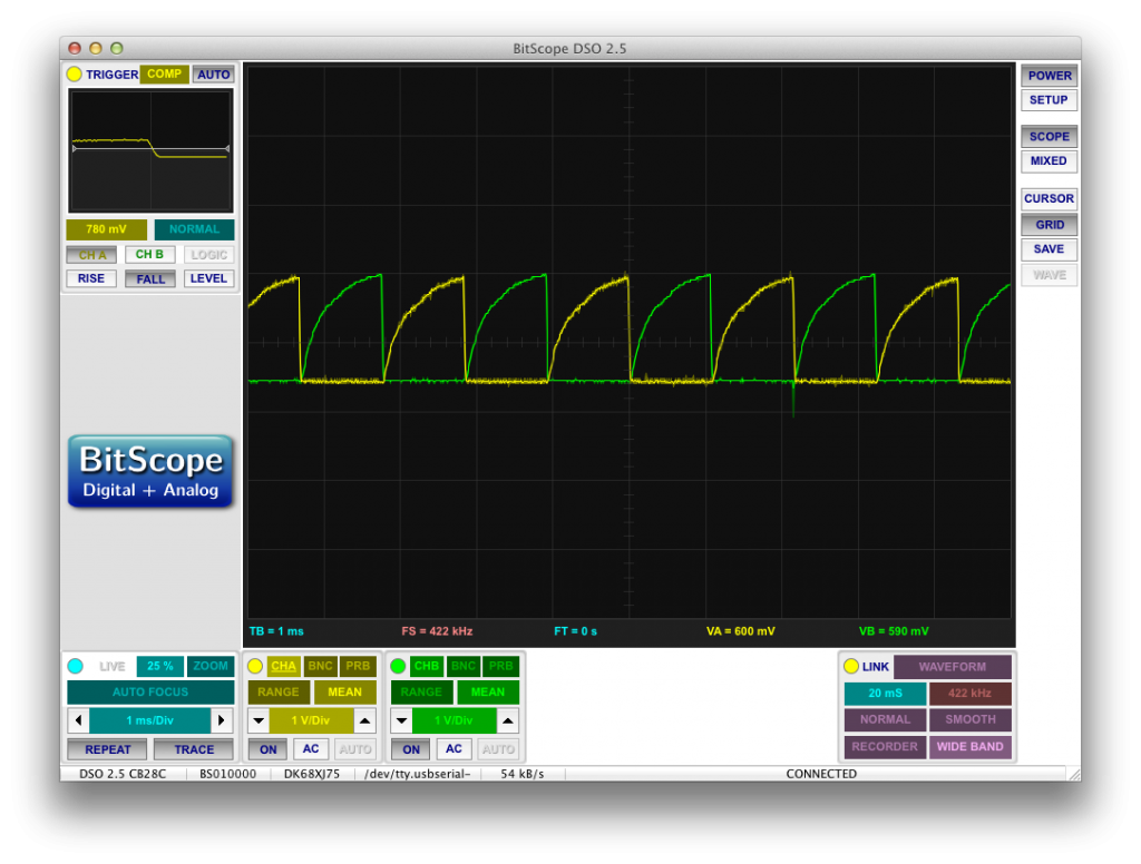
If you look at the voltages of each side of the EL panel (one side in green and the other in yellow), you’ll see that they both drop to zero at every H-bridge transition:
Yet we saw from before that the DC rail never drops below 45. So at some point, there is a 45V difference between the high side voltage rail and the EL panel terminal that it’s supposed to be powering. You can actually see this difference clearly here: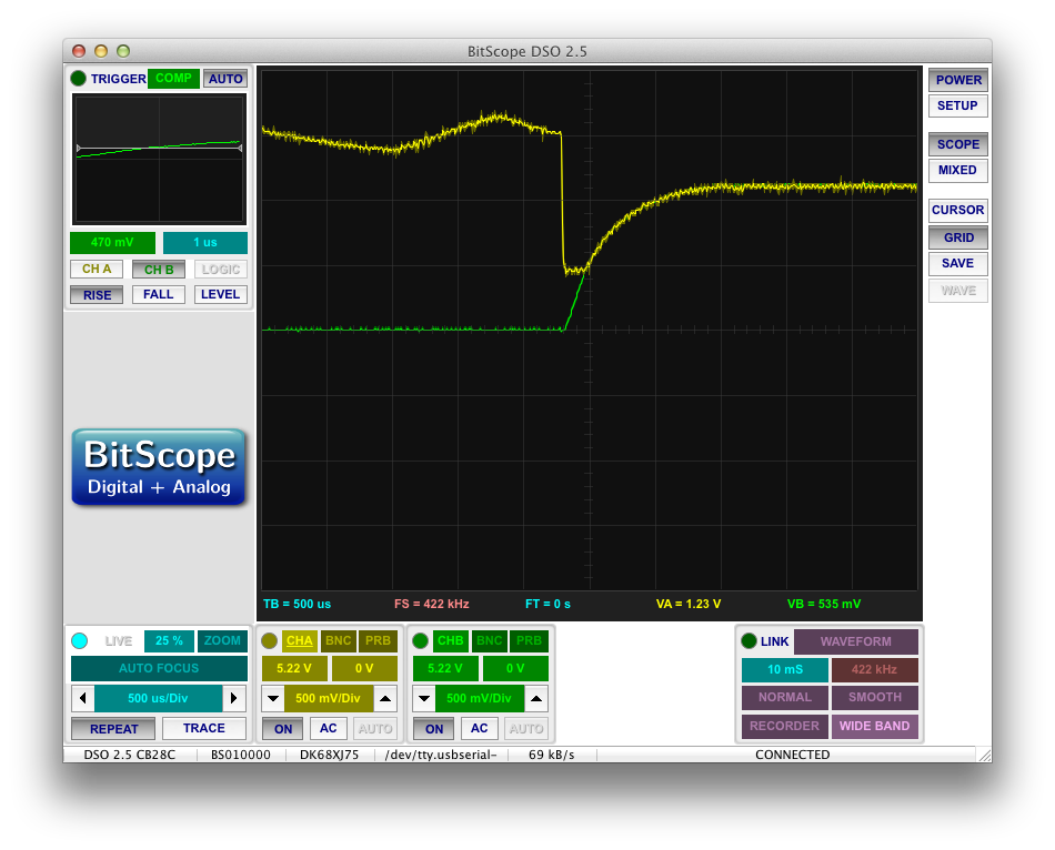
When it comes time to raise that EL rail (green), the DC rail (yellow) droops to 45V and then rises only after the EL rail itself rises at about 45V.
So how can this circuit maintain this 45V discrepancy? Looking at my H-bridge schematic doodle above, it would appear that the EL rail should be connected directly to the DC rail. This actually isn’t the case. Instead of four switches in my H-bridge, I’m using four FETs: two NFETS on the low side and two PFETs on the high side. As you’ll see, these PFETs are far from ideal switches.
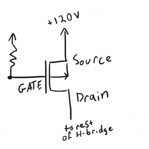
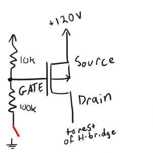
Driving these PFETs was kind of tricky because of how large my voltage rail is. In my schematic, I tied the PFET’s source to the high side rail as usual.
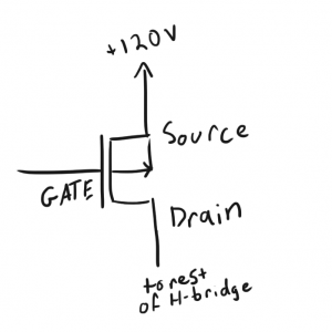 To turn the PFET off, I have a pull-up resistor pulling the gate to the high side rail.
Normally, you would turn a PFET on by pulling down on its gate; as the gate voltage drops further and further below the source voltage, the FET will allow more current to flow from source to drain.
Unfortunately, this wasn’t possible here because if I were to pull the gate down to ground (say with an NFET), I would end up with an extremely large gate-source voltage (
![]()
) which would damage the FET. To solve this problem, I simply added another resistor of a larger value to the gate setting up a voltage divider that would make
![]()
about
![]()
th of the DC voltage rail.
As long as
![]()
is sufficiently large, the PFET will conduct current into my H-bridge and into my EL panel. The problem arises when the rail voltage starts to sag. As that rail starts to sag, the amount of voltage dropped across the high-side resistor (and therefore
![]()
) starts to shrink. At some point,
![]()
gets so small that the PFET will start to shut off and limit the amount of current passing from source to drain.
So the rail voltage would probably drop all the way to zero if it weren’t for the fact that the PFET starts to prevent my bypass capacitor from sourcing any more current to the H-bridge.
This sets up a sort of feedback system. Any additional current being provided by the flyback converter will travel into the bypass capacitor and attempt to raise the DC rail (and the source voltage). This rising source voltage will cause
![]()
to rise as well which will turn on the PFET and cause it to suck the new current out of the bypass capacitor.
This cycle will continue until enough current has passed through the PFET to raise the EL panel voltage up to about 40-ish Volts. At this point, the drain Voltage of the PFET will approach the bypass capacitor voltage and the new current will no longer be sucked into the PFET exclusively allowing both the EL panel voltage and DC rail voltage to rise together as you can see in the image above.
Just to test this theory, I replaced one of my pull up resistors with a resistor of a larger value. That means that when that PFET is on, the DC voltage rail should be able to droop much lower (larger pull up resistor means larger
![]()
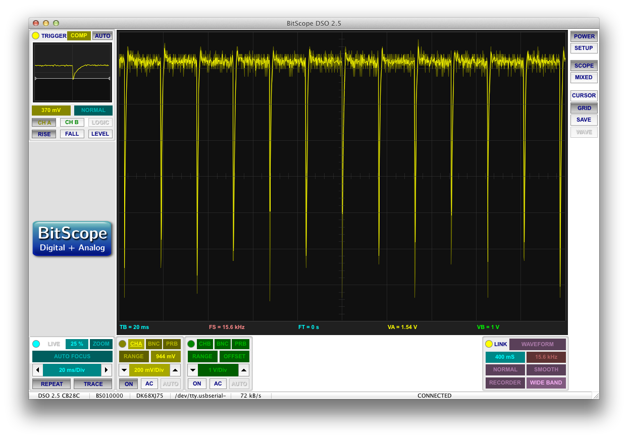
). You can actually see this happening in the following scope trace of the DC rail:
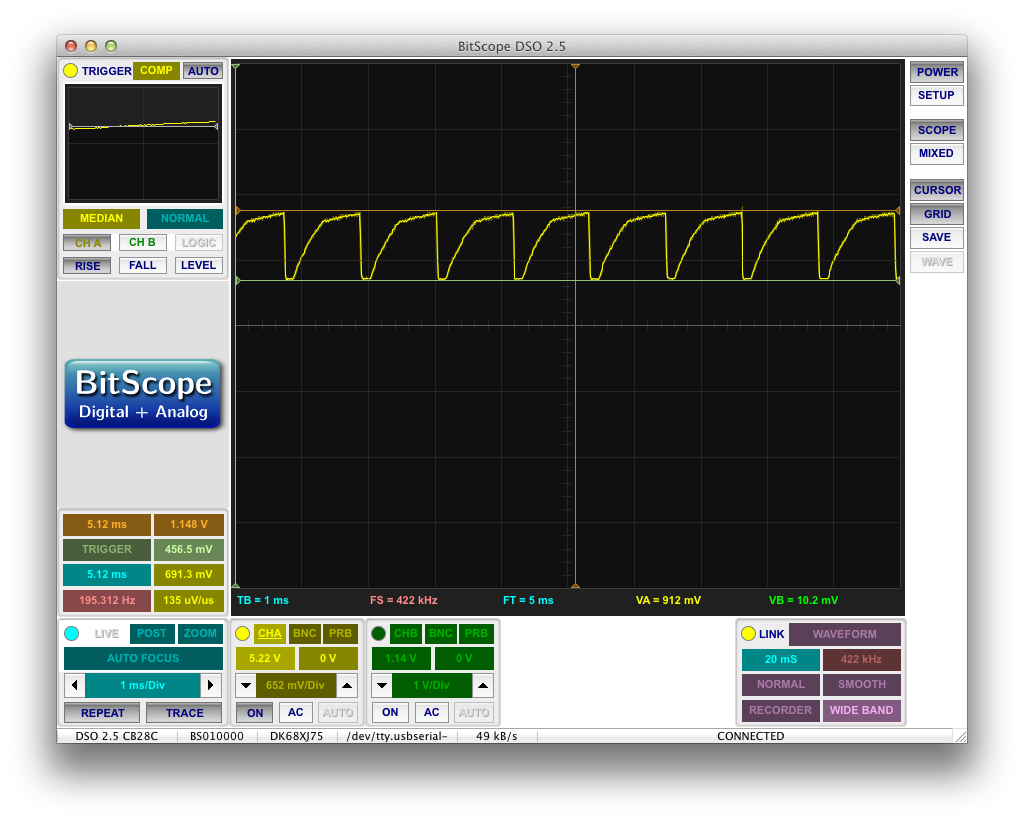
Every time my modified PFET is turned on, the voltage drops a little lower than when the unmodified PFET is turned on. Because they alternate, you see a lovely decorative icicle effect in the above trace.
Why No Negative?
We’ve established in the previous section that the PFET is shutting off prior to the DC rail dropping all the way to zero and that both sides of the EL wire drop to zero every cycle. The question is: where does the charge come from?
As I said before, because the EL panel is negatively charged, it requires current just to reach a zero charge state. So where is this charge coming from if the PFET is shut off?
You also have to remember that there’s an NFET pulling the positively charged side of the EL panel down to ground, so the negatively charged side (the side under the PFET) should be at a negative potential.
But if we look at that plot from before, at no point do my EL panel terminals drop below 0V, so if the PFET is off, what the heck is keeping this terminal from going negative?
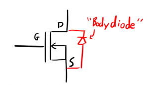
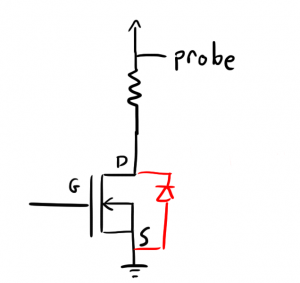
As it turns out, it’s that other low-side switch that’s supposed to act as an open circuit. If you connect an NFET such that the source is at a higher potential than the drain, current will freely flow even if the NFET is turned off. This is a result of the “body diode” that exists in FETs. We usually don’t talk about the body diode because it’s rarely used, but it’s basically a result of the way FETs are made.
So while this rail would love to go negative, the body diode of the turned off NFET will conduct charge from the ground plane into the EL panel pulling it up to ground potential. It’s almost like I infringed on that patent by accident!
So, if my theory is correct, there should be an enormous amount of current flowing backwards through this FET while it’s shut off. To measure this, I put a 10
![]()
current sensing resistor between the NFET’s drain and the rest of the circuit.
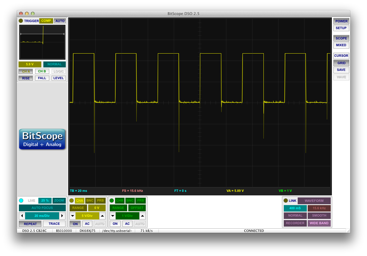
We should expect to see a negative voltage spike as current passes from ground into the EL panel through the body diode. The larger this current, the larger the voltage drop across the resistor and the larger the voltage spike.
Keep in mind that the positive-going voltage swings actually go all the way up to 120V, but my scope truncates them.
So there you have it folks! Negative spikes!
SCIENCE
Conclusion
So if I knew the solution right away, was I wasting my time writing this post? I don’t think so. I think I learned a lot from this bug, and I had a lot of fun solving it.
Looking forward, I think the real lesson is that sizing components for a power supply meant to drive something as strange as an EL panel is a lot more complicated than a typical load.
I’ll probably end up just accepting a slightly dimmer max brightness on this supply, but rebuilding the power supply from scratch is another option. Its design was riddled with miscalculations and I’ve had a host of other problems. My transformer never had the requisite retention clip, and for some reason, my nominal output voltage suddenly rose from 120V to 150V and I can’t figure out why. It may have something to do with all of the messy reworks I’ve done of this circuit. In fact, it’s likely that the efficiency boost I got from using the body diodes is the only reason my EL panel got as bright as it did.
I think in the future, I’ll calculate the current draw of an EL panel based on its size and expected power draw and try to size my components for that. Hopefully I’ll end up with a smaller power supply that gets the job done with none of the whine.
Continue the story here.



Pingback: Revisiting the EL Panel and the True Meaning of RMS | ch00ftech Industries
Pingback: Naw But Really Though…How Do You Power An EL Panel? | ch00ftech Industries
Pingback: Sound Reactive EL Panel Dimmer (for real this time) | ch00ftech Industries
You need an LC filter between each half bridge and the EL to lighten the FETs’ loads and to eliminate this problem. The L will allow the drain voltages to change while little current flows. The voltage will start current flowing in the inductors. The current will continue to flow briefly through the body diodes after the switches open. The capacitors to ground smoothe out the transients.
Dude, this is literally one of the best write-ups on a electronics issue I’ve every seen on the WWW. Mad props. Clearly explained, and nice graphs and hand drawn schematics. Not to mention extremely interesting! We have been having issues with H-bridge EL drives, and I realized we were missing the resistor divider for the P-Channel gate drive! (it was just being pulled to ground, exceeding the negative gate-source maximum voltage, causing gate punch-through, and then the P-Channel failing close-circuit).
Pingback: A while back I found this cool EL panel hack when I was looking for a graphic eq | Reactive Lights
Thanks for citing a reference to a model of EL devices. Unfortunately it looks to be a model with no parameter values. Any ideas about the values of Ci, Cp, and the zener breakdown voltages in the model? These obviously vary with the area of the wire or panel, but it would be great to have some quantitative estimates.
From EL manufacturers I have found estimates of panel capacitance, and series and parallel resistance. For example a large tape project I’m considering would be 360nF, 14.5Ω and 24.7kΩ.
I’m wondering if there is anything to gain in my LTspice simulation from replacing my current EL model (simply a cap with the series and parallel resistances) with the model you cited.
I honestly have no idea what those values should be, and I’ve found that they vary dramatically from vendor to vendor. I’ve never really had much luck simulating an EL wire circuit, so I don’t have much I can offer there either.
I’d be excited to see what you come up with though.
Here’s another excellent reference on the topic: http://eecs.oregonstate.edu/matdev/pub/hitt-modelingreview.pdf
It doesn’t get me any closer to a working model in LTspice, but it identifies some of the folks working in the area and cites a lot of literature. I’ve asked to author for advice on how to translate the physics into a practical model. Fingers crossed.
The same authors have published on the aging of EL products. Wouldn’t it be great to know how to minimize aging by tweaking the power supply?
Pingback: xX_MLG_Keyboard_Xx #SWAG #YOLO #420 | ch00ftech Industries