When this whole EL wire obsession started, I was a little disappointed with the poor efficiency I was getting out of my cheap Chinese EL wire drivers. I assumed that they (like a lot of things coming out of China) were poorly designed.
I was wrong.
Background
This post will be one of two where I completely debunk a previous post I made about EL wire. If you’ve been following the blog, this has become kind of a trend.
The post in question is this one. In it, I dissected some EL wire power supplies that I purchased off Amazon. Not only was the build quality atrocious (one of them was dead on arrival due to an obviously bad solder joint), but they also had design flaw where a temporary power disconnection (bump) would cause a brown-out on the onboard micro controller that could only be fixed by pulling out a battery. Taking these apart, I was expecting to find a lesson in “what not to do”.
Considering I bought five of these and 50 feet of wire for less than  35 instead of <$10, that’s not surprising. I quickly set about taking it apart and seeing how it worked.
What I found was shocking. Not only did this dimming power supply contain inside it a run-of-the-mill blocking oscillator (instead of some space-age crap like I tried to make), it had the exact same design as my crappy supplies. With similar component values!
I was very surprised that another (better) designer with no relation to the first chose this similar design that I assumed was inferior. Clearly, this required more investigation.
Repeating the Experiment
Looking back, I noticed a few flaws with my previous experiment:
- I never disconnected the micro-controller from the Chinese power supply. This micro-controller is only necessary to control the blinking modes that the supply offers and only served to waste current during my test.
- I wasn’t powering the two supplies at the same voltage. Each supply runs off of two 1.5V cells, but I made no attempt to ensure that they were at the exact same level of charge.
- I wasn’t quantifying the outputs. I only compared the two outputs by how brightly they appeared to illuminate the EL wire.
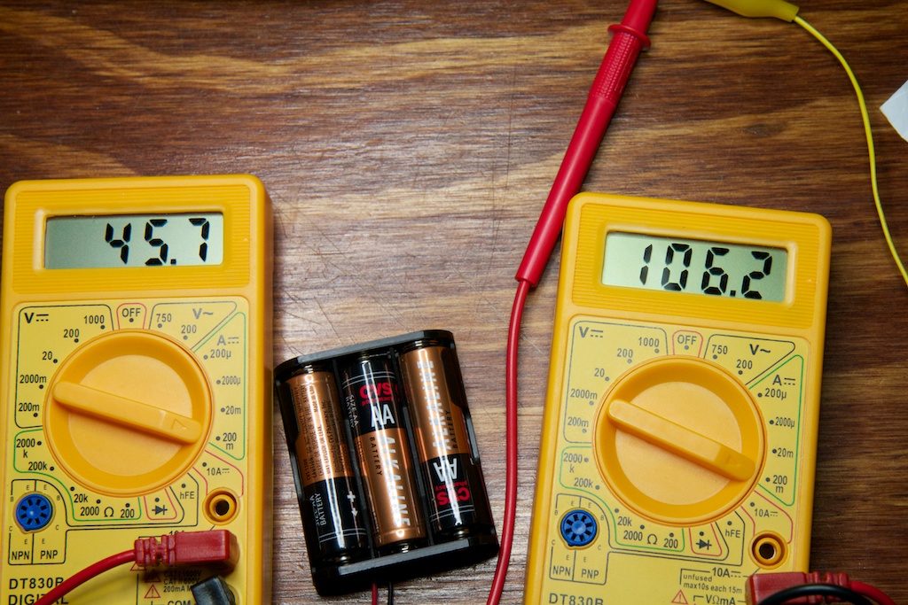
To make the experiment a little more valid, I ran it again with both supplies hooked up to the same voltage source (some AA batteries). I measured the input current as well as the output voltage. I forgot to take a picture of the output voltage readings, but for my input current, I got this:
Where my supply is the one drawing 45mA. It would appear that my supply is much more efficient considering it draws less than half the current and makes the EL wire look similarly bright:
However, this is where the quantification comes in. My supply was only putting out 73.8V at 4.68kHz while the Chinese supply put out a whopping 95.3V at 3.47kHz with similar loads. I’ve discovered that measuring power output into EL wire is difficult due to it being a reactive load (more on this in another post), however, since power draw usually scales as V
![]()
, I can give the relative power output of the two supplies:
![]()
So it looks like the Chinese supply is outputting 1.66 times the power that my supply is putting out. Now let’s calculate power draw using P=V
![]()
I:
![]()
The Chinese supply draws 2.35x the power of of my supply but it delivers much less than that to the load, so my supply is still more efficient. I’m not certain exactly what role output frequency plays on output power but can assume that higher frequency is more power (EL wire gets brighter), and considering my supply puts out a higher frequency, that’s even more damning.
Going to Simulation
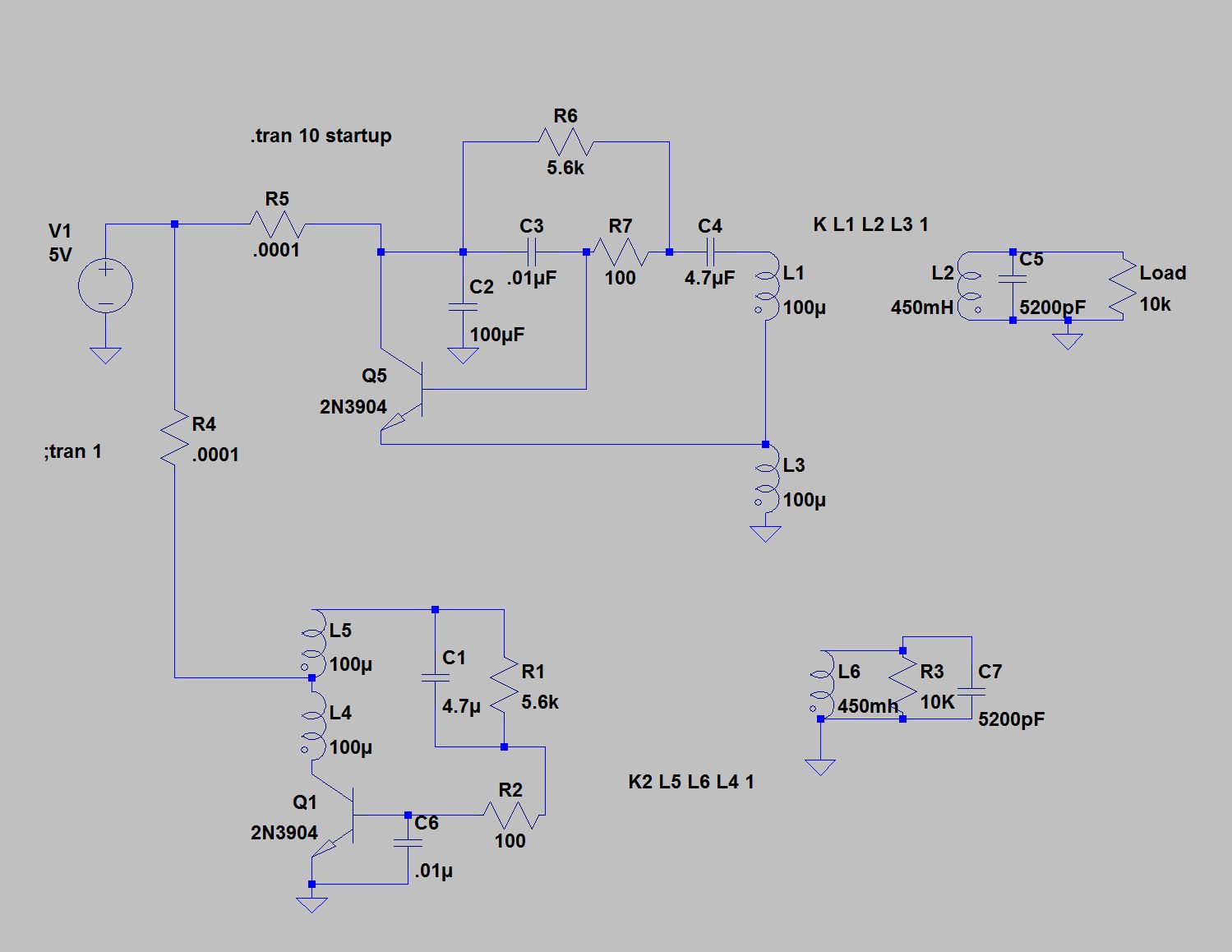
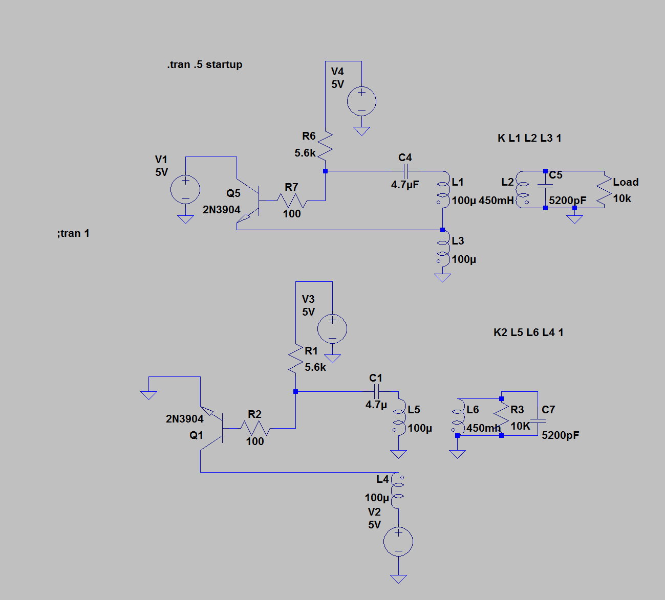
At this point, I thought it might be interesting to try my spice simulation again, but this time being more careful to match the component values to isolate the differences to the topology alone. I came up with this:
It might be a little tricky to tell them apart, but the top circuit is the Chinese design while the bottom is mine. Plotting the output voltage (across L2 and L6), I got this:
THEY WERE EXACTLY THE SAME!
This really surprised me. How could these two very different topologies give the exact same output? It was at about this time that I decided to ask reddit for some help. Unfortunately, I had about a bazillion questions and probably should have organized my thoughts better before bugging them. As a result, I got a number of annoyed replies, but I did glean some very helpful information from the thread.
One user pointed how how sensitive these particular oscillator topologies are to component values. Because of this, it was unfair of me to compare the Chinese supply’s topology to my own when they were using drastically different components. For example, it could just be that the Chinese supply has a crappy transistor or phantom loads that are draining power.
To further isolate variables, I ran a new experiment.
Test Two
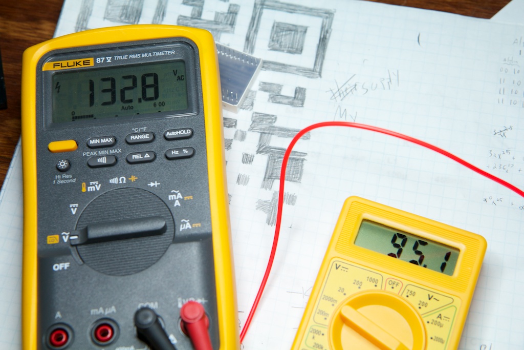
I grabbed some components and a breadboard and set to work building both supplies. I made it a point to build one supply, measure it, take it apart, and build the other out of the same components so that there would be no effects from slight variations between parts. First up is my supply:
Not too bad. 132V output with a 95.1mA current draw at 5V. This time I was running at a higher input voltage so it makes sense that the output is higher. Now for their supply:
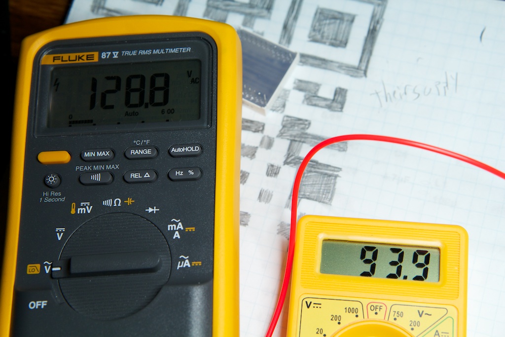
Remarkably similar! On top of that, they both put out approximately 4.6kHz.
Full disclosure, I did have to change a single value between these two supplies. C3 and C6 are used to reduce super high speed ringing on the base of the BJT. I discovered their importance when I built my first supply. In order to get both of these oscillators to work, I had to use a different cap for each of them. My design used a .1
![]()
F while theirs used .01
![]()
F. Considering the LTSpice model actually doesn’t require this capacitor at all, I’m assuming changing it only affects stability and not efficiency.
Alright, so apparently these two topologies perform about the same and my previous judgements about the Chinese design are completely unfounded. So this brings up another question: How do they act the same but look so different?
Are They Really That Different?
Another reddit user pointed out to me that the two topologies really aren’t that different. Skeptical, I decided to move a few things around as he suggested. I came up with this:
A few notes about why I am able to do what I did:
- As I said before, C3 and C6 are only needed in the real world and can be removed in simulation.
- C2 was acting as a bypass capacitor which is not needed when my simulated power supply has zero output impedance.
- R5 and R4 were never really part of the circuit and were only in place to make it easier to measure the current going to each node in LTSpice.
- L5’s output is passed through a DC blocking capacitor. Because of this, it doesn’t necessarily have to be tied to the V+ rail. Because it’s only passing an AC signal through that capacitor, It’ll work as long as it’s tied to something at a fixed potential. In this case, ground.
- Unlike L5, R1 still does need to be connected to the V+ rail. It passes a small amount of DC current into the oscillator to get it started and keep it going. Previously it was passing the DC component of the current through L5, but now that L5 has been moved, it needs a connection of its own.
So with those changes, you can see the the two oscillators look very similar indeed. Besides the obvious difference that the main voltage source and ground are hooked up to opposite ends, the only real difference is the connection of L1 and L5. L5 is connected to ground, but making the same connection to L1 will halt the oscillator.
AC-DC
To better understand what’s going on here, it’s important to do some AC and DC analysis. This is something that I never had a very good grasp of in college, and it’s really coming back to bite me in the ass.
With most analog circuits like this, you can split their currents into AC and DC components and analyze them separately to see how the circuit performs. With DC analysis, you assume that all inductors are shorts (wire) and all capacitors are opens. Then with AC analysis, you do the opposite. I sort of already did this in my bullet list above when I moved R5. An AC signal would short through C1 and go around R5 and a DC signal would travel straight from V+ through L5 to R5 as if it were tied directly to V+. Moving R5 didn’t change its AC nor DC behavior, so it could be moved freely without affecting anything.
Looking at this circuit with DC analysis will let us determine the bias current passing through the base of the BJT. An NPN BJT will pass more current from collector to emitter if more current is passed from its base to emitter. The exact relationship isn’t linear though. For example, the change in collector current between 1 and 2mA of base current might be much larger or smaller than the change between 2 and 3mA.
For any very small changes though, it’s usually safe to assume that the device is linear. i.e. the difference between 1.9-2mA might be close to the difference between 2-2.1mA. This is where the bias current comes in. If two transistors are at the same bias point, they will perform similarly to small wiggles around that point (which are part of the AC signal).
So, if you do your DC analysis above and turn all the inductors into shorts and all the capacitors into opens, you’ll see that each transistor’s emitter is tied to ground and base is tied to V+ through a 100
![]()
and 5.6k
![]()
resistor. They’re at the same DC bias point. I can expect them to behave very similarly to small “wiggles” on their base.
Now what about the AC analysis?
The “wiggling” around the base is produced by the inductors L1 and L5. These two inductors are getting their currents through induction from the other windings of their transformers. Because they’re getting their power “wirelessly”, they can be moved around the circuit and still behave similarly. The question is, why can’t L1 be grounded like L5?
AC analysis tells us that L5 is connected in series with the 100
![]()
resistor, and the two are connected to the base and emitter of Q1. In order for the AC analysis to be the same on L1, it must also be connected through its 100
![]()
resistor to the base and emitter of its Q2. Because its BJT’s emitter is not tied to ground, L1 can’t be grounded. It has to be tied to the emitter directly.
So if you look at these two circuits from an AC and DC perspective, they are exactly the same.
So Which is Better?
In short: I still don’t know.
My goal with my recent investigation was to try to determine which supply is better. In theory, they’re both exactly the same, but I can imagine that there might be minor benefits of one over the other when practical considerations are taken into account.
The real lesson here is that my design is not overwhelmingly better as previously thought. Given that the theory doesn’t point to either topology as a winner, the only basis on which I have to base my opinion is …someone else’s opinion.
Apparently the two people who designed my two store-bought supplies chose the same design, so without more extensive research, humbly, I think I’m going to just use that topology from now on. All the cool kids are doing it after all.
Continue the story here.



Pingback: EL Wire is Spanish for…The Wire | ch00ftech Industries
Pingback: Method #1,571 For Not Dimming An EL Panel: TRIAC | ch00ftech Industries
Very interesting article. I really should get better at my AC and DC analysis and not rely so much on simulations. 🙂
I’m just a rank amateur when it comes to stuff, but I still find your posts fascinating. I don’t understand the details, but I really enjoy how you lay out your process, what steps you take and why.
One of the two designs is less sensitive to low-battery-voltage than the other.
One of the two designs is less sensitive to low-transistor-beta than the other, as someone on reddit already pointed out. The LTSPICE model of a 2N4401 represents a *typical* device, not a just-barely-achieves-the-min-Beta-spec part.
One of the two designs has got higher Q at its small-signal operating point, than the other design (because the impedances at the transistor ports load the LC networks differently). The design with higher Q is less sensitive to non-idealities in the inductors and capacitors. It is better able to tolerate higher winding resistance, larger coil-to-coil capacitance, and earlier core saturation than the other design.
And there are other sensitivities to consider: Sensitivity to temperature. Sensitivity to output load (e.g. what happens if some dunce runs the oscillator without connecting any EL wire as a load?). Sensitivity to variations in EL wire distributed parameters (C per unit length, R per unit C) when you change from one mfr’s EL wire to another mfr’s EL wire.
All very interesting points!
As I said, I’m pretty weak in the analog realm, and I’ve got all the info I need for now, but I will definitely be returning to your points in the future.
Thank you.
Pingback: Dimming EL Wire Dreamcatcher | ch00ftech Industries
Great info. Have you found simple or complex solution for the brown out?
I ended up just removing the micro controller entirely and shorting together the proper contacts to make it turn on all the time.
If you have the time, would you mind posting a picture of what you did? The PCB picture in your article “El Wire is Spanish for…” was detailed and It would be super helpful if I could see how you altered it. I’ve just added EL Wire to my bike and I’ve run into the same brown out problem for the nighttime commute home. Thanks.
I’m not sure if that would help. These supplies are all a little different, so the layout will be different between mine and yours. What they do all seem to have in common is that there is a high side PFET that controls current going into the power supply segment.
Here’s what you should do. Solder a piece of wire to the negative terminal of your batteries, then tap the other end of that wire to each pin of the micro controller. Be careful because some of these pins will short out the batteries, so don’t hold it there long. When the EL wire lights up, you’ve got it right (be careful how you hold the circuit though, you might get quite a shock!).
If this doesn’t work, shoot me an email using the link at the top of the site with more details/images. I’d like to help you find a solution and add it to my oft neglected “reader mail” section of the site.
I appreciate the info. I’m more of a biker and not so strong with circuits and electronics so I’ll brush up on that and get back to you. For starters I’ll have to identify the micro controller. It’s something I definitely want to try out because I bike to work and it’s getting darker much earlier. Will keep you posted. Thanks.
Pingback: Sound Reactive EL Panel Dimmer (for real this time) | ch00ftech Industries